
Datasheet

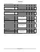

NTHD4508N
http://onsemi.com
5
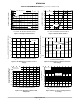
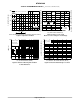
Figure 11. Basic Figure 12. Style 2
0.457
0.018
2.032
0.08
0.635
0.025
0.66
0.026
0.254
0.010
mm
inches
SCALE 20:1
1.032
0.043
0.178
0.007
0.457
0.018
2.032
0.08
0.635
0.025
0.66
0.026
0.711
0.028
*For additional information on our Pb−Free strategy and soldering
details, please download the ON Semiconductor Soldering and
Mounting Techniques Reference Manual, SOLDERRM/D.
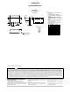
SOLDERING FOOTPRINTS*
BASIC PAD PATTERNS
The basic pad layout with dimensions is shown in
Figure 11. This is sufficient for low power dissipation
MOSFET applications, but power semiconductor
performance requires a greater copper pad area, particularly
for the drain leads.
The minimum recommended pad pattern shown in Figure
12 improves the thermal area of the drain connections (pins
5, 6, 7, 8) while remaining within the confines of the basic
footprint. The drain copper area is 0.0019 sq. in. (or 1.22 sq.
mm). This will assist the power dissipation path away from
the device (through the copper lead−frame) and into the
board and exterior chassis (if applicable) for the single
device. The addition of a further copper area and/or the
addition of vias to other board layers will enhance the
performance still further.