
Datasheet


PmodCLP™ Reference Manual
Copyright Digilent, Inc. All rights reserved.
Other product and company names mentioned may be trademarks of their respective owners.
Page 2 of 6
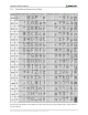
Header J1 - Top Half
Header J1 - Bottom Half
Header J2
Pin
Signal
Description
Pin
Signal
Description
Pin
Signal
Description
1
DB0
Data Bit 0
7
DB4
Data Bit 4
1
RS
Register Select: High for
Data Transfer, Low for
Instruction Transfer
2
DB1
Data Bit 1
8
DB5
Data Bit 5
2
R/W
Read/Write signal: High
for Read mode, Low for
Write mode
3
DB2
Data Bit 2
9
DB6
Data Bit 6
3
E
Read/Write Enable: High
for Read, falling edge
writes data
4
DB3
Data Bit 3
10
DB7
Data Bit 7
4
NC
Optional back-light
enable (not connected on
the PmodCLP
5
GND
Power Supply
Ground
11
GND
Power Supply
Ground
5
GND
Power Supply Ground
6
VCC
Positive
Power
Supply
1
12
VCC
Positive
Power Supply¹
6
VCC
Positive Power Supply
Table 1. PmodCLP Connector Signals.
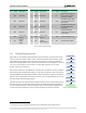
2.1 Timing Requirements
After power-on, at least 20ms must elapse before the “Function Set” instruction code can be
written to set the bus width, number of lines, and character patterns (8-bit interface, 2 lines,
and 5×8 dots are appropriate). After the Function Set instruction, at least 37us must elapse
before the “Display On/Off Control” instruction can be written (to turn the display on, turn the
cursor on or off, and set the cursor to blink or no blink). After another 37us, the “Clear
Display” instruction can be issued.
After another 1.52ms, the “Entry Mode Set” instruction can set address increment (or address
decrement) mode, and display shift mode (on or off). After this sequence, data can be written
into the DDRAM via the “Write data into RAM” to cause information to appear on the display.
Note that other compatible LCD controllers use similar start-up sequences which may not use
the same timings as the Samsung controller.
The table below lists the required bit order needed in order to send a variety of instructions to
the LCD controller on the PmodCLP. Before the 8 bits of parallel data (DB7 through DB0) are
sent, the output enable pin, E, must be brought to a high '1' state and then brought to a low
'0' state at end of the sequence in order to transfer the data bits to the LCD controller.
1
For Revision A of the PmodCLP this must be at 5V. For Revision B, this must be at 3.3V
Power On
Wait 20ms
Set Function
Wait 37 us
Display Set
Wait 37 us
Display Clear
Wait 1.52ms
OK
Figure 1. LCD startup sequence.