
Datasheet


Basys 3™ FPGA Board Reference Manual
Copyright Digilent, Inc. All rights reserved.
Other product and company names mentioned may be trademarks of their respective owners.
Page 17 of 19
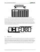
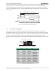
in digit position 1. Then, if AN1 is asserted while CA, CB, and CC are asserted, a "7" will be displayed in digit
position 2. If AN0, CB, and CC are driven for 4ms, and then AN1, CA, CB, and CC are driven for 4ms in an endless
succession, the display will show "71" in the first two digits. An example timing diagram for a four-digit controller is
shown in Fig. 19.
AN0
AN1
AN2
AN3
Cathodes
Digit 0
Refresh period = 1ms to 16ms
Digit period = Refresh / 4
Digit 1 Digit 2 Digit 3
Figure 19. Four digit scanning display controller timing diagram.
9 Pmod Controllers
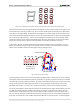
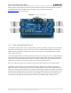
The Pmod connectors are arranged in a 2x6 right-angle, and are 100-mil female connectors that mate with
standard 2x6 pin headers. Each 12-pin Pmod connector provides two 3.3V VCC signals (pins 6 and 12), two Ground
signals (pins 5 and 11), and eight logic signals, as shown in Fig. 20. The VCC and Ground pins can deliver up to 1A of
current. Pmod data signals are not matched pairs, and they are routed using best-available tracks without
impedance control or delay matching. Pin assignments for the Pmod I/O connected to the FPGA are shown in Table
6.
Pin 1
Pin 12
Pin 6
8 signalsVCC GND
Figure 20. Pmod connectors; front view as loaded on PCB.
Pmod JA
Pmod JB
Pmod JC
Pmod XDAC
JA1: J1
JB1: A14
JC1: K17
JXADC1: J3
JA2: L2
JB2: A16
JC2: M18
JXADC2: L3
JA3: J2
JB3: B15
JC3: N17
JXADC3: M2
JA4: G2
JB4: B16
JC4: P18
JXADC4: N2
JA7: H1
JB7: A15
JC7: L17
JXADC7: K3
JA8: K2
JB8: A17
JC8: M19
JXADC8: M3
JA9: H2
JB9: C15
JC9: P17
JXADC9: M1
JA10: G3
JB10: C16
JC10: R18
JXADC10: N1
Table 6. Basys 3 Pmod pin assignment.