ENC424J600/624J600 Data Sheet Stand-Alone 10/100 Ethernet Controller with SPI or Parallel Interface 2010 Microchip Technology Inc.
Note the following details of the code protection feature on Microchip devices: • Microchip products meet the specification contained in their particular Microchip Data Sheet. • Microchip believes that its family of products is one of the most secure families of its kind on the market today, when used in the intended manner and under normal conditions. • There are dishonest and possibly illegal methods used to breach the code protection feature.
ENC424J600/624J600 Stand-Alone 10/100 Ethernet Controller with SPI or Parallel Interface • • • • • • • • • • • • • • • IEEE 802.
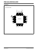
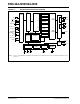
ENC424J600/624J600 Pin Diagrams VSS PSPCFG0 AD14 AD13 AD12 AD11 AD10 AD9 AD8 INT/SPISEL CLKOUT 44-Pin TQFP and QFN 33 32 31 30 29 28 27 26 25 24 23 CS/CS SO/WR/EN SI/RD/RW SCK/AL AD0 AD1 AD2 AD3 VSS VCAP VDD 34 35 36 37 38 39 40 41 42 43 44 ENC424J600 22 21 20 19 18 17 16 15 14 13 12 VSSTX TPOUTTPOUT+ VSSTX VDDTX TPINTPIN+ VDDRX VSSRX VSSPLL VDDPLL VSSOSC OSC2 OSC1 VDDOSC AD4 AD5 AD6 AD7 LEDB LEDA RBIAS 1 2 3 4 5 6 7 8 9 10 11 DS39935C-page 2 2010 Microchip Technology Inc.
ENC424J600/624J600 Pin Diagrams (Continued) CLKOUT INT/SPISEL AD8 AD9 AD10 AD11 AD12 AD13 AD14 AD15 A12 A14/PSPCFG1 A13 VSS VDD WRH/B1SEL 64-Pin TQFP 48 47 46 45 44 43 42 41 40 39 38 37 36 35 34 33 CS/CS SO/WR/WRL/EN/B0SEL 49 32 VSSTX 50 31 TPOUT- SI/RD/RW 51 30 TPOUT+ SCK/AL/PSPCFG4 AD0 52 29 53 28 AD1 AD2 54 27 VSSTX VDDTX TPIN- 55 26 TPIN+ AD3 56 25 A0 57 A1 A2 A3 58 23 VDDRX VSSRX VSSPLL 59 22 VDDPLL 60 21 VDD A4 VSS 61 20 62 19 A11 A10 VCAP V
ENC424J600/624J600 Table of Contents 1.0 Device Overview .......................................................................................................................................................................... 5 2.0 External Connections ................................................................................................................................................................... 9 3.0 Memory Organization ...................................................................
ENC424J600/624J600 1.0 DEVICE OVERVIEW This document contains device-specific information for the following devices: • ENC424J600 • ENC624J600 Communication with the microcontroller is implemented via the SPI or parallel interface, with data rates ranging from 14 Mbit/s (SPI) to 160 Mbit/s (demultiplexed, 16-bit parallel interface). Dedicated pins are used for LED link and activity indication and for transmit/receive/DMA interrupts.
ENC424J600/624J600 FIGURE 1-1: ENC424J600/624J600 BLOCK DIAGRAM Bus Interface CS/CS SCK/AL SI/RD/RW m3 m0 m1 PHY TPOUT+ DMA and Checksum MII Interface TX TPOUT- TPIN+ RX TPINm2 Parallel WR/WRL/ EN/B0SEL(1) MAC Crypto Cores AD<15:0>(1) A<14:0>(1) RX Control Logic RX Filter Common SO Arbiter SPI I/O Interface TX Control Logic Flow Control Memory WRH/ B1SEL(1) Control Registers SRAM 24 Kbytes MIIM Interface RBIAS Host Interface PSPCFGx(1) SPISEL 25 MHz Oscillator Control Logic IN
ENC424J600/624J600 TABLE 1-2: ENC424J600/624J600 PINOUT DESCRIPTIONS Pin Number Pin Type Input Buffer 53 I/O CMOS 39 54 I/O CMOS 40 55 I/O CMOS AD3 41 56 I/O CMOS AD4 5 5 I/O CMOS AD5 6 6 I/O CMOS AD6 7 7 I/O CMOS Pin Name 44-Pin 64-Pin AD0 38 AD1 AD2 AD7 8 8 I/O CMOS AD8 25 35 I/O CMOS AD9 26 36 I/O CMOS AD10 27 37 I/O CMOS AD11 28 38 I/O CMOS AD12 29 39 I/O CMOS AD13 30 40 I/O CMOS AD14 31 41 I/O CMOS AD15 — 42 I/O CMOS
ENC424J600/624J600 TABLE 1-2: Pin Name ENC424J600/624J600 PINOUT DESCRIPTIONS (CONTINUED) Pin Number Pin Type Input Buffer ANA 44-Pin 64-Pin 3 3 I OSC1 Description 25 MHz Crystal Oscillator/Clock Input OSC2 2 2 O — PSPCFG0 32 — I CMOS PSP Mode Select 0 PSPCFG1 — 45 I CMOS PSP Mode Select 1 PSPCFG2 — 17 I CMOS PSP Mode Select 2 PSPCFG3 — 18 I CMOS PSP Mode Select 3 PSPCFG4 — 52 I CMOS PSP Mode Select 4 RBIAS 11 16 I ANA RD 36 51 I CMOS PSP Read Strobe
ENC424J600/624J600 2.0 EXTERNAL CONNECTIONS 2.1 Oscillator When clocking the device using a crystal, follow the connections shown in Figure 2-1. When using a CMOS clock oscillator or other external clock source, follow Figure 2-2. CRYSTAL OSCILLATOR OPERATION ENCX24J600 C1 (3) OSC1 To Internal Logic XTAL RF(2) C2(3) EXTERNAL CLOCK SOURCE ENCX24J600 ENC424J600/624J600 devices are designed to operate from a fixed 25 MHz clock input.
ENC424J600/624J600 2.3 2.3.1 Voltage and Bias Pin FIGURE 2-3: VDD AND VSS PINS 3.3V To reduce on-die noise levels and provide for the high-current demands of Ethernet, there are many power pins on ENC424J600/624J600 devices: • • • • • VDD and VSS VDDOSC and VSSOSC VDDPLL and VSSPLL VDDRX and VSSRX VDDTX and VSSTX Each VDD and VSS pin pair above should have a 0.1 F ceramic bypass capacitor placed as close to the pins as possible. For best EMI emission suppression, other smaller capacitors, such as 0.
ENC424J600/624J600 2.4 Ethernet Signal Pins and External Magnetics Typical applications for ENC424J600/624J600 devices require an Ethernet transformer module, and a few resistors and capacitors to implement a complete IEEE 802.3 compliant 10/100 Ethernet interface, as shown in Figure 2-5. The Ethernet transmit interface consists of two pins: TPOUT+ and TPOUT-. These pins implement a differential pair and a current-mode transmitter.
ENC424J600/624J600 2.4.1 ADDITIONAL EMI AND LAYOUT CONSIDERATIONS To reduce EMI emissions, common-mode chokes are shown adjacent to the transformers on the cable (RJ-45) side. These chokes come standard in typical Ethernet transformer modules. Because the ENCX24J600 PHY uses a current-mode drive topology, the transmit choke must normally be located on the cable side of the transmit transformer.
ENC424J600/624J600 2.6 INT Pin The INT pin is an active-low signal that is used to flag interrupt events to external devices. Depending on the application, it can be used to signal the host microcontroller whenever a packet has been received or transmitted, or that some other asynchronous operation has occurred. It can also be used to wake-up the microcontroller or other system components based on LAN activity; its use is optional.
ENC424J600/624J600 2.7.1 SPI parallel interfaces; not all available pins are used in every configuration. Up to 8 different operating modes are available. These are explained in detail in Section 5.0 “Parallel Slave Port Interface (PSP)”. When enabled, the SPI interface is implemented with four pins: • • • • CS SO SI SCK All four of these pins must be connected to use the SPI interface. The PSPCFG pins control which parallel interface mode is used.
ENC424J600/624J600 2.7.3 CS/CS PIN The chip select functions for the serial and parallel interfaces are shared on one common pin, CS/CS. This pin is equipped with both internal weak pull-up and weak pull-down resistors. If the SPI interface is selected (CS), the pull-up resistor is automatically enabled and the pull-down resistor is disabled. If the PSP interface is chosen (CS), the pull-down resistor is automatically enabled and the pull-up resistor is disabled.
ENC424J600/624J600 NOTES: DS39935C-page 16 2010 Microchip Technology Inc.
ENC424J600/624J600 3.0 MEMORY ORGANIZATION 3.1.1 SPI INTERFACE MAP All memory in ENC424J600/624J600 devices is implemented as volatile RAM.
ENC424J600/624J600 3.1.2 PSP INTERFACE MAPS When one of the parallel interfaces is selected, the memory map is very different from the SPI map. There are two different memory address spaces (Figure 3-2): • the main memory area • the PHY register area As in the serial memory map, the main memory area is a linear, byte-addressable space of 32 Kbytes, with the SRAM buffer located in the first 24-Kbyte region. The cryptographic data memory is also mapped to the same location as in the serial memory map.
ENC424J600/624J600 3.2 Special Function Registers The SFRs provide the main interface between the host controller and the on-chip Ethernet controller logic. Writing to these registers controls the operation of the interface, while reading the registers allows the host controller to monitor operations. All registers are 16 bits wide.
ENC424J600/624J600 TABLE 3-1: ENC424J600/624J600 SFR MAP (SPI INTERFACE) Bank 2 (40h offset) Unbanked(1) (80h offset) Bank 3 (60h offset) ETXSTL 01 01 ETXSTH 21 EHT1H 41 MACON1H 61 MAADR3H 81 Reserved 02 02 ETXLENL 22 EHT2L 42 MACON2L 62 MAADR2L 82 ERXDATA(2) 03 03 ETXLENH 23 EHT2H 43 MACON2H 63 MAADR2H 83 Reserved 04 04 ERXSTL 24 EHT3L 44 MABBIPGL 64 MAADR1L 84 EUDADATA(2) 20 EHT1L 40 MACON1L Name Unbanked Address 00 Name Unbanked Address 00 Name
ENC424J600/624J600 3.2.4 PSP REGISTER MAP When using a PSP interface, the SFR memory is linear; all registers are directly accessible without banking. To maintain consistency with the SPI interface, the EUDAST, EUDAND, ESTAT, EIR and ECON1 registers are instantiated in four locations in the PSP memory maps. Users may opt to use any one of these four locations. TABLE 3-2: Addr The SFR maps for the 8-bit and 16-bit PSP interfaces are shown in Table 3-2 and Table 3-3, respectively.
ENC424J600/624J600 TABLE 3-3: ENC424J600/624J600 SFR MAP (BASE REGISTER MAP, 16-BIT PSP INTERFACE) Addr Name Addr Name Addr Name Addr Name Addr Name 3F00 ETXST 3F10 EHT1 3F20 MACON1 3F30 MAADR3 3F40 EGPDATA 3F01 ETXLEN 3F11 EHT2 3F21 MACON2 3F31 MAADR2 3F41 ERXDATA 3F02 ERXST 3F12 EHT3 3F22 MABBIPG 3F32 MAADR1 3F42 EUDADATA 3F03 ERXTAIL 3F13 EHT4 3F23 MAIPG 3F33 MIWR 3F43 EGPRDPT 3F04 ERXHEAD 3F14 EPMM1 3F24 MACLCON 3F34 MIRD 3F44 EGPWRPT 3F05 E
ENC424J600/624J600 TABLE 3-4: ENC424J600/624J600 SFR MAP (SET REGISTER MAP, 8-BIT PSP INTERFACE) Bit Set Registers (7F00h to 7F7Fh)(1) Addr Name Addr Name Addr Name Addr Name 7F00 ETXSTSETL 7F20 EHT1SETL 7F40 Reserved 7F60 Reserved 7F01 ETXSTSETH 7F21 EHT1SETH 7F41 Reserved 7F61 Reserved 7F02 ETXLENSETL 7F22 EHT2SETL 7F42 Reserved 7F62 Reserved 7F03 ETXLENSETH 7F23 EHT2SETH 7F43 Reserved 7F63 Reserved 7F04 ERXSTSETL 7F24 EHT3SETL 7F44 Reserved 7F64 Reserved
ENC424J600/624J600 TABLE 3-5: ENC424J600/624J600 SFR MAP (CLR REGISTER MAP, 8-BIT PSP INTERFACE) Bit Clear Registers (7F80h to 7FFFh)(1) Addr Name Addr Name Addr Name Addr Name 7F80 ETXSTCLRL 7FA0 EHT1CLRL 7FC0 Reserved 7FE0 Reserved 7F81 ETXSTCLRH 7FA1 EHT1CLRH 7FC1 Reserved 7FE1 Reserved 7F82 ETXLENCLRL 7FA2 EHT2CLRL 7FC2 Reserved 7FE2 Reserved 7F83 ETXLENCLRH 7FA3 EHT2CLRH 7FC3 Reserved 7FE3 Reserved 7F84 ERXSTCLRL 7FA4 EHT3CLRL 7FC4 Reserved 7FE4 Reserved
ENC424J600/624J600 TABLE 3-6: ENC424J600/624J600 SFR MAP (SET/CLR REGISTER MAP, 16-BIT PSP INTERFACE) Bit Set Registers (3F80h to 3FBFh)(1) Addr Name Addr Name Addr Name Addr Name 3F80 ETXSTSET 3F90 EHT1SET 3FA0 Reserved 3FB0 Reserved 3F81 ETXLENSET 3F91 EHT2SET 3FA1 Reserved 3FB1 Reserved 3F82 ERXSTSET 3F92 EHT3SET 3FA2 Reserved 3FB2 Reserved 3F83 ERXTAILSET 3F93 EHT4SET 3FA3 Reserved 3FB3 Reserved 3F84 — 3F94 EPMM1SET 3FA4 Reserved 3FB4 Reserved 3F85 EDMA
High Byte (‘H’ Register) 8-Bit File Name ENC424J600/624J600 REGISTER FILE SUMMARY Bit 7 16-Bit Bit 15 Low Byte (‘L’ Register) Bit 6 Bit 5 Bit 4 Bit 3 Bit 2 Bit 1 Bit 0 Bit 14 Bit 13 Bit 12 Bit 11 Bit 10 Bit 9 Bit 8 Bit 7 Bit 6 Bit 5 Bit 4 Bit 3 Bit 2 Bit 1 Bit 0 Bit 7 Bit 6 Bit 5 Bit 4 Bit 3 Bit 2 Bit 1 Bit 0 EUDAST — User-Defined Area Start Pointer (EUDAST<14:8>) User-Defined Area Start Pointer (EUDAST<7:0>) EUDAND — User-Defined Area End Pointer (EUDAND<14:8>) U
2010 Microchip Technology Inc.
ENC424J600/624J600 3.3 PHY Special Function Registers The PHY registers provide configuration and control of the PHY module, as well as status information about its operation. These 16-bit registers are located in their own memory space, outside of the main SFR space. Unlike other SFRs, the PHY SFRs are not directly accessible through the SPI or PSP interfaces.
ENC424J600/624J600 3.3.3 SCANNING A PHY REGISTER The MAC can be configured to perform automatic back-to-back read operations on a PHY register. This can reduce the host controller complexity when periodic status information updates are desired. To perform the scan operation: 1. 2. Write the address of the PHY register to read from into the MIREGADR register. Make sure to also set reserved bit 8 of this register. Set the MIISCAN (MICMD<1>) bit.
ENC424J600/624J600 REGISTER 3-2: MICMD: MII MANAGEMENT COMMAND REGISTER U-0 U-0 U-0 U-0 U-0 U-0 U-0 U-0 — — — — — — — — bit 15 bit 8 U-0 U-0 U-0 U-0 U-0 U-0 R/W-0 R/W-0 — — — — — — MIISCAN MIIRD bit 7 bit 0 Legend: R = Readable bit W = Writable bit U = Unimplemented bit, read as ‘0’ -n = Value at POR ‘1’ = Bit is set ‘0’ = Bit is cleared x = Bit is unknown bit 15-2 Unimplemented: Read as ‘0’ bit 1 MIISCAN: MII Scan Enable bit 1 = PHY register designated by MIR
2010 Microchip Technology Inc.
ENC424J600/624J600 3.4 Cryptographic Data Memory The cryptographic data memory is used to store key and data information for the Modular Exponentiation, AES and MD5/SHA-1 hashing engines. The RAM for these modules is actually implemented inside of the modules themselves; this allows fast memory access for the access-intensive encryption engines, as well as the simultaneous use of more than one module by an application.
ENC424J600/624J600 3.5.1 GENERAL PURPOSE BUFFER The general purpose buffer memory starts at address 0000h and includes all memory up to, but not including, the memory address pointed to by the ERXST register (i.e., ERXST – 1). This buffer can be used to store transmit packets, received data that the host controller wishes to save for an extended period, or any type of volatile or state information that the host controller does not have room internally to save.
ENC424J600/624J600 3.5.5 INDIRECT SRAM BUFFER ACCESS Indirect access to the SRAM buffer is available to all I/O interfaces. For the SPI interface, it is the only method available. For PSP interfaces, it may be used in addition to the direct access method.
ENC424J600/624J600 For example, to read data from address 5402h of the buffer: 1. 2. Write 5402h to EGPRDPT. Read from EGPDATA. Following the read, the EGPRDPT value normally increments by 1 (to 5403h in this example). If the host subsequently wants to read from address 5403h, it can simply perform a second read from the EGPDATA Window register. The Write Pointer, EGPWRPT, is not affected by the read operation. Similarly, to write A3h to address 0007h of the buffer: 1. 2. Write 0007h to EGPWRPT.
ENC424J600/624J600 3.5.5.2 Circular Wrapping with ERXDATA FIGURE 3-7: As with the general purpose pointers, operations with ERXDATA normally cause the ERXRDPT or ERXWRPT Pointer to automatically increment by one byte address. However, if the end of the receive buffer area (5FFFh) is reached, the pointer will increment to the start of the receive FIFO buffer area instead, as defined by ERXST (Figure 3-7).
ENC424J600/624J600 The user-defined area start address, EUDAST, is a read/write register. For wrapping to work correctly, the hardware enforces 16-bit even word alignment of this register by internally having the Least Significant bit tied off to ‘0’. Similarly, the user-defined area end address, EUDAND, is a read/write register that is forced to an odd memory address. The Least Significant bit of EUDAND is internally tied to ‘1’.
ENC424J600/624J600 NOTES: DS39935C-page 38 2010 Microchip Technology Inc.
ENC424J600/624J600 4.0 SERIAL PERIPHERAL INTERFACE (SPI) ENC424J600/624J600 devices implement an optional SPI I/O port for applications where a parallel microcontroller interface is not available or is undesirable. An SPI port is commonly available on many microcontrollers, and can be simulated in software on regular I/O pins where it is not implemented. This makes the SPI port ideal for using ENC424J600/624J600 devices with the widest possible range of host controllers. 4.
ENC424J600/624J600 TABLE 4-1: SPI INSTRUCTION SET Instruction Mnemonic Instruction 1st Byte 2nd Byte 3rd Byte Nth Byte Bank 0 Select B0SEL 1100 0000 — — — Bank 1 Select B1SEL 1100 0010 — — — Bank 2 Select B2SEL 1100 0100 — — — Bank 3 Select B3SEL 1100 0110 — — — System Reset SETETHRST 1100 1010 — — — Flow Control Disable FCDISABLE 1110 0000 — — — Flow Control Single FCSINGLE 1110 0010 — — — Flow Control Multiple FCMULTIPLE 1110 0100 — — — Flow Control C
ENC424J600/624J600 4.3 Single Byte Instructions 4.3.1 The bank select opcodes, B0SEL, B1SEL, B2SEL and B3SEL, switch the SFR bank to Bank 0, Bank 1, Bank 2 or Bank 3, respectively. The updated bank select state is saved internally inside the ENCX24J600 in volatile memory. Firmware can retrieve the currently selected SFR bank state by using the Read Bank Select (RBSEL) opcode. All single byte instructions are designed to perform a simple command that affects the ENCX24J600 device’s state.
ENC424J600/624J600 TABLE 4-2: SINGLE BYTE INSTRUCTIONS Mnemonic Opcode Instruction B0SEL 1100 0000 Selects SFR Bank 0 B1SEL 1100 0010 Selects SFR Bank 1 B2SEL 1100 0100 Selects SFR Bank 2 B3SEL 1100 0110 Selects SFR Bank 3 SETETHRST 1100 1010 Issues System Reset by setting ETHRST (ECON2<4>) FCDISABLE 1110 0000 Disables flow control (sets ECON1<7:6> = 00) FCSINGLE 1110 0010 Transmits a single pause frame (sets ECON1<7:6> = 01) FCMULTIPLE 1110 0100 Enables flow control with periodic pause
ENC424J600/624J600 4.5 Three-Byte Instructions For write commands (shown in Figure 4-4), the opcode byte (‘011xxx00’) must be presented on the SI line, MSb first, followed immediately by the pointer data to be written. Like the data returned during a read operation, the write data must be presented MSb first, Least Significant Byte first. All three-byte instructions are designed to quickly read or update the Read and Write Pointers used to access the SRAM buffer area.
ENC424J600/624J600 TABLE 4-3: Mnemonic THREE-BYTE INSTRUCTIONS Opcode Argument 3rd Byte Instruction 1st Byte 2nd Byte WGPRDPT 0110 0000 dddd dddd DDDD DDDD Write General Purpose Buffer Read Pointer (EGPRDPT). RGPRDPT 0110 0010 xxxx xxxx XXXX XXXX Read General Purpose Buffer Read Pointer (EGPRDPT). WRXRDPT 0110 0100 dddd dddd DDDD DDDD Write Receive Buffer Read Pointer (ERXRDPT). RRXRDPT 0110 0110 xxxx xxxx XXXX XXXX Read Receive Buffer Read Pointer (ERXRDPT).
ENC424J600/624J600 4.6 N-Byte Instructions bank prior to their execution. Because of this, they cannot be used for the unbanked SFR space (80h through 9Fh). N-byte instructions make up the most versatile class of SPI commands, as they can read or write to any addressable SFR or SRAM space. Their name comes from their variable length nature; they require a minimum of two bytes, but can take an indefinite number of bytes of data argument, or return an unlimited number of output bytes.
ENC424J600/624J600 There are four banked SFR opcodes, summarized in Table 4-4. Additional details for these opcodes are provided below. 4.6.1.1 WCR Opcode The Write Control Register (WCR) opcode byte consists of the prefix, ‘010’, concatenated with the 5-bit banked SFR address of the first register to write to. For example, if Bank 3 were currently selected and the host microcontroller wanted to write to the ECON2L register at banked address 0Eh, the 8-bit opcode would be ‘01001110’ or 4Eh.
ENC424J600/624J600 4.6.2 UNBANKED SFR OPERATIONS byte-wise on SO, MSb first. As with three-byte instructions, the lower byte of a data word is presented first, followed by the upper byte. The N-byte unbanked SFR instructions are WCRU, RCRU, BFSU and BFCU. These instructions use an opcode with a one-byte address argument and do not depend on the use of BxSEL instructions for SFR bank selection.
ENC424J600/624J600 4.6.2.1 WCRU Opcode The Write Control Register Unbanked (WCRU) opcode starts with the opcode, ‘00100010’ (22h), followed by the unbanked SFR register address during SPI clocks, 9 through 16. For example, to write to ECON2L at address 6Eh, the instruction would be ‘22h 6Eh’, followed by the data to be written. When the host controller is finished writing data, it should raise the CS line, putting the device in an inactive state and preparing it for the next SPI instruction.
ENC424J600/624J600 4.6.3 SRAM BUFFER OPERATIONS SO during SCK clocks, 1 through 8. Starting with the 9th clock, data is clocked out byte-wise on SO, MSb first. The six N-byte SRAM instructions function in a similar manner to the banked SFR instructions, in that they use a single byte opcode to define the operation and target register. In terms of timing, they are virtually identical, as shown in Figure 4-7.
ENC424J600/624J600 TABLE 4-6: N-BYTE SRAM INSTRUCTIONS Instruction Mnemonic Opcode Argument 1st Byte 2nd Byte 3rd Byte Nth Byte Read Data from EGPDATA RGPDATA 0010 1000 xxxx xxxx XXXX XXXX XXXX XXXX Write Data from EGPDATA WGPDATA 0010 1010 dddd dddd DDDD DDDD DDDD DDDD Read Data from ERXDATA RRXDATA 0010 1100 xxxx xxxx XXXX XXXX XXXX XXXX Write Data from ERXDATA WRXDATA 0010 1110 dddd dddd DDDD DDDD DDDD DDDD Read Data from EUDADATA RUDADATA 0011 0000 xxxx xxxx XXXX XXX
ENC424J600/624J600 5.0 PARALLEL SLAVE PORT INTERFACE (PSP) ENC424J600/624J600 devices are designed to interface directly with the parallel port available on many microcontrollers, including the Parallel Master Port (PMP) available on many Microchip PIC® microcontrollers. The Parallel Slave Port interface is highly flexible, and can communicate using either Intel® or Motorola® formats for read and write control strobes.
ENC424J600/624J600 5.2 Using the PSP Interface Unlike the serial interface, the PSP interface does not use opcodes or a command architecture to control the device. Instead, the memory space is accessed directly using the addressing schemes described in Section 3.1.2 “PSP Interface Maps”. Control SFRs are read and written to directly, or manipulated through their accompanying Bit Set and Bit Clear registers. In 16-bit modes, each address (from 0 to 16,384) points to a different word.
ENC424J600/624J600 5.2.5 PERFORMANCE CONSIDERATIONS When using a 16-bit data bus width, all registers and direct access to SRAM can be accomplished through 16-bit accesses. Therefore, these modes are potentially twice as fast as their 8-bit equivalent parallel mode. However, accesses through the hardware-managed SRAM read/write registers, EGPDATA, ERXDATA and EUDADATA, are always 8-bit regardless of the interface used.
ENC424J600/624J600 FIGURE 5-1: DEVICE CONNECTIONS FOR PSP MODE 1 Host MCU ENC624J600 CS(1) RD WR PMCSx PMRD PMWR 6 PMA<14:9> PMA<8:0> 8 PMD<7:0> INTx A<14:9>(2) A<8:0> 9 AD<7:0> (3) INT/SPISEL 100 k PSPCFG2 PSPCFG3 PSPCFG4 Note 1: Use of the CS strobe from the controller is optional. If not used, tie CS to VDD. 2: Connect these pins when direct addressing of the entire SRAM buffer is required. Tie to VDD when only indirect addressing is desired.
ENC424J600/624J600 5.3.2 MODE 2 To perform a read operation: PSP Mode 2 is also an 8-bit, fully demultiplexed mode that is available on 64-pin devices only. The parallel interface consists of 8 bidirectional data pins (AD<7:0>) and 9 to 15 separate address pins (A<14:0>). To select PSP Mode 2, tie PSPCFG2 and PSPCFG3 to VSS, while connecting PSPCFG4 to VDD. Figure 5-4 demonstrates connections required to use Mode 2. 1. 2. 3.
ENC424J600/624J600 FIGURE 5-5: MODE 2 READ OPERATION TIMING (TWO BYTES) CS R/W EN TPSP1 A<14:0> AD<7:0> TPSP4 Address<14:0> Hi-Z Data<7:0> TPSP2 FIGURE 5-6: Address<14:0> Hi-Z Data<7:0> Hi-Z TPSP3 MODE 2 WRITE OPERATION TIMING (TWO BYTES) CS TPSP5 R/W EN TPSP8 A<14:0> AD<7:0> DS39935C-page 56 TPSP6 Address<14:0> Hi-Z TPSP7 Data<7:0> TPSP11 TPSP9 Address<14:0> TPSP10 Data<7:0> Hi-Z 2010 Microchip Technology Inc.
ENC424J600/624J600 5.3.3 MODE 3 When RD is raised high, the data bus begins driving out indeterminate data for a brief period, then switches to the correct read data after the appropriate read access time has elapsed. When the RD strobe is lowered, the data pins will return to a high-impedance state. PSP Mode 3 is a 16-bit, fully demultiplexed mode that is available on 64-pin devices only.
ENC424J600/624J600 FIGURE 5-8: MODE 3 READ OPERATION TIMING (FOUR BYTES) CS RD TPSP1 TPSP4 WRL WRH Address<13:0> A<13:0> Hi-Z AD<15:0> Data<15:0> TPSP2 FIGURE 5-9: Address<13:0> Hi-Z Data<15:0> Hi-Z TPSP3 MODE 3 WRITE OPERATION TIMING (THREE BYTES) CS TPSP5 RD WRL TPSP8 TPSP11 WRH A<13:0> AD<15:0> DS39935C-page 58 TPSP6 Address<13:0> Hi-Z TPSP7 Data<15:0> TPSP9 Address<13:0> TPSP10 Data<7:0> Hi-Z 2010 Microchip Technology Inc.
ENC424J600/624J600 5.3.4 MODE 4 4. When either BxSEL pin is raised high, the data bus begins driving out indeterminate data for a brief period, then switches to the correct read data after the appropriate read access time has elapsed. When B0SEL and B1SEL are both low, the data bus pins return to a high-impedance state. PSP Mode 4 is also a 16-bit, fully demultiplexed mode that is available in 64-pin devices only.
ENC424J600/624J600 FIGURE 5-11: MODE 4 READ OPERATION TIMING (FOUR BYTES) CS R/W B0SEL T PSP1 TPSP4 B1SEL A<13:0> AD<15:0> Address<13:0> Hi-Z Data<15:0> TPSP2 FIGURE 5-12: Address<13:0> Hi-Z Data<15:0> Hi-Z TPSP3 MODE 4 WRITE OPERATION TIMING (THREE BYTES) CS TPSP5 R/W B0SEL TPSP8 TPSP11 B1SEL TPSP6 Address<13:0> A<13:0> AD<15:0> DS39935C-page 60 Hi-Z TPSP7 Data<15:0> TPSP9 Address<13:0> TPSP10 Data<7:0> Hi-Z 2010 Microchip Technology Inc.
ENC424J600/624J600 5.3.5 MODE 5 To perform a write operation: PSP Mode 5 is an 8-bit, partially multiplexed mode that is available on all devices. The parallel interface consists of 8 multiplexed address and data pins (AD<7:0>), plus one required high address bit (AD8) and 6 optional address-only pins (AD<14:9>). 1. 2. 3. 4. Raise CS (if connected to the host). Present the address to write to on AD<14:0>. Strobe the AL pin.
ENC424J600/624J600 FIGURE 5-13: 44-pin Devices: DEVICE CONNECTIONS FOR PSP MODE 5 Host MCU ENC424J600 PMCSx PMRD PMWR PMALL PMA<14:9> PMA8 PMD<7:0> CS(1) RD WR AL 6 AD<14:9>(2) AD8 AD<7:0> 8 INTx(3) INT/SPISEL 100 k PSPCFG0 64-pin Devices: Host MCU ENC624J600 (1) CS RD WR AL PMCSx PMRD PMWR PMALL PMA<14:9> PMA8 PMD<7:0> 6 AD<14:9>(2) AD8 AD<7:0> 8 INTx(3) INT/SPISEL +3.3V 100 k PSPCFG1 PSPCFG2 PSPCFG3 Note 1: Use of the CS strobe from the controller is optional.
ENC424J600/624J600 FIGURE 5-14: MODE 5 READ OPERATION TIMING (TWO BYTES – SAME ADDRESS) CS TPSP12 RD TPSP4 WR AL TPSP13 AD<14:9>(1) Address<14:9> AD8(1) AD<7:0> TPSP15 Address<8> Hi-Z Address<7:0> TPSP12 Data<7:0> TPSP2 Hi-Z Data<7:0> Hi-Z TPSP3 TPSP14 Note 1: AD8 must be driven by the host controller. AD<14:9> may be tied to logic high when only indirect access is desired.
ENC424J600/624J600 5.3.6 MODE 6 To perform a read operation: PSP Mode 6 is also an 8-bit, partially multiplexed mode that is available on all devices. The parallel interface consists of 8 multiplexed address and data pins (AD<7:0>), plus one required high address bit (AD8) and 6 optional address-only pins (AD<14:9>). 1. 2. 3. 4. Selecting PSP Mode 6 differs between 44-pin and 64-pin devices, as shown in Figure 5-16. For the 44-pin ENC424J600, tie PSPCFG0 to VDD.
ENC424J600/624J600 FIGURE 5-16: DEVICE CONNECTIONS FOR PSP MODE 6 44-pin Devices: Host MCU ENC424J600 PMCSx PMRD/PMWR PMENB PMALL PMA<14:9> PMA8 PMD<7:0> CS(1) R/W EN AL 6 AD<14:9>(2) AD8 AD<7:0> 8 INTx(3) INT/SPISEL +3.3V 100 k PSPCFG0 64-pin Devices: Host MCU ENC624J600 CS(1) R/W EN AL PMCSx PMRD/PMWR PMENB PMALL PMA<14:9> PMA8 PMD<7:0> 6 AD<14:9>(2) AD8 AD<7:0> 8 INTx(3) INT/SPISEL +3.3V 100 k Note 1: PSPCFG1 PSPCFG2 PSPCFG3 Use of the CS strobe from the controller is optional.
ENC424J600/624J600 FIGURE 5-17: MODE 6 READ OPERATION TIMING (TWO BYTES – SAME ADDRESS) CS T PSP12 R/W T PSP1 EN T PSP4 AL T PSP13 AD<14:9> (1) Address<14:9> AD8 (1) AD<7:0> T PSP15 Address<8> Hi-Z Address<7:0> Data<7:0> T PSP12 T PSP2 Hi-Z Data<7:0> Hi-Z T PSP3 T PSP14 Note 1: AD8 must be driven by the host controller. AD<14:9> may be tied to logic high when only indirect access is desired .
ENC424J600/624J600 5.3.7 MODE 9 The AD<15:0> bus begins driving out indeterminate data for a brief period, then switches to the correct read data after the appropriate read access time has elapsed. When RD is lowered, the AD<15:0> pins return to a high-impedance state. PSP Mode 9 is a 16-bit, fully-multiplexed mode that is available on 64-pin devices only. The parallel interface consists of 16 bidirectional data pins (AD<15:0>); the lower 14 (AD<13:0>) also function as address pins.
ENC424J600/624J600 FIGURE 5-20: MODE 9 READ OPERATION TIMING (FOUR BYTES – SAME ADDRESS) CS TPSP12 RD TPSP4 WRL WRH AL AD<15:0> TPSP13 Hi-Z Address<13:0> TPSP12 FIGURE 5-21: TPSP15 TPSP14 Data<15:0> TPSP2 Hi-Z Data<15:0> Hi-Z TPSP3 MODE 9 WRITE OPERATION TIMING (THREE BYTES – SAME ADDRESS) CS TPSP12 RD WRL TPSP8 TPSP11 WRH AL AD<15:0> TPSP13 Hi-Z Address<13:0> TPSP12 DS39935C-page 68 TPSP14 Data<15:0> TPSP7 Data<7:0> Hi-Z TPSP10 2010 Microchip Technology Inc.
ENC424J600/624J600 5.3.8 MODE 10 When either BxSEL pin is raised high, the AD<15:0> bus begins driving out indeterminate data for a brief period, then switches to the correct read data after the appropriate read access time has elapsed. When B0SEL and B1SEL are both low, AD<15:0> return to a high-impedance state. PSP Mode 10 is also a 16-bit, fully-multiplexed mode that is available on 64-pin devices only.
ENC424J600/624J600 FIGURE 5-23: MODE 10 READ OPERATION TIMING (FOUR BYTES – SAME ADDRESS) CS T PSP12 R/W TPSP1 B0SEL T PSP4 B1SEL AL AD<15:0> TPSP13 Hi-Z Address<13:0> T PSP12 FIGURE 5-24: T PSP15 T PSP14 Data<15:0> T PSP2 Hi-Z Data<15:0> Hi-Z TPSP3 MODE 10 WRITE OPERATION TIMING (THREE BYTES – SAME ADDRESS) CS T PSP12 R/W T PSP5 B0SEL T PSP8 TPSP11 B1SEL AL AD<15:0> TPSP13 Hi-Z Address<13:0> TPSP12 DS39935C-page 70 T PSP14 Data<15:0> TPSP7 Data<7:0> Hi-Z TPSP10 2010
ENC424J600/624J600 6.0 ETHERNET OVERVIEW 6.1.1 Before discussing the use of ENC424J600/624J600 devices in Ethernet applications, it may be helpful to review the structure of a typical data frame. For more detailed information, refer to IEEE 802.3 Standard, which defines the Ethernet protocol, or to Microchip Application Note AN1120, “Ethernet Theory of Operation”. 6.
ENC424J600/624J600 If the Least Significant bit in the first byte of this address is set (i.e., the byte is odd), the address is a Multicast destination. From the previous example, 01-00-BA-BE-F0-0D and 33-45-DE-AD-BE-EF are Multicast addresses. Multicast frames are designated for use by a selected group of Ethernet nodes. The Multicast address, FF-FF-FF-FF-FF-FF, is reserved; it is known as the Broadcast address and is directed to all nodes on the network.
ENC424J600/624J600 7.0 RESET 7.2 ENC424J600/624J600 differentiates between five types of Resets: • • • • • Power-on Reset (POR) System Reset Transmit Only Reset Receive Only Reset PHY Subsystem Reset A simplified block diagram of the on-chip Reset circuit is shown in Figure 7-1. 7.1 Power-on Reset Power-on Reset occurs when VDD rises above VPOR. This allows the device to start in the initialized state when VDD is adequate for the device’s digital logic to operate correctly.
ENC424J600/624J600 7.3 Transmit Only Reset A Transmit Only Reset is performed by setting the TXRST bit (ECON2<6>). The transmit logic is held in Reset until the bit is cleared. Any pending transmission is aborted and TXRTS (ECON1<1>) is cleared. To resume normal operation, clear the TXRST bit. Both the POR and System Resets automatically perform a Transmit Reset, so this step does not need to be performed after a System or Power-on Reset. Only the transmit logic is affected by this operation.
ENC424J600/624J600 8.0 INITIALIZATION Before using an ENCX24J600 device to transmit and receive packets, certain device settings must be initialized. Depending on the application, some configuration options may be left set to their default values. Those that need to be changed are typically set once after power-up and not changed thereafter. 8.
ENC424J600/624J600 8.6.1 PREPROGRAMMED MAC ADDRESS As shipped, each ENCX24J600 device has been preprogrammed with a unique MAC address. This value is stored in nonvolatile memory and reloaded into the MAADR registers after every Power-on and System Reset. The factory preprogrammed MAC address is permanent and will be restored to the MAC registers after each Reset. The preprogrammed address in nonvolatile memory cannot be changed by the user, but it can be overwritten in the SFRs.
ENC424J600/624J600 REGISTER 8-1: ECON2: ETHERNET CONTROL REGISTER 2 R/W-1 R/W-1 R/W-0 R/W-0 R/W-1(1) R/W-0(1) R/W-1(1) R/W-1(1) ETHEN STRCH TXMAC SHA1MD5 COCON3 COCON2 COCON1 COCON0 bit 15 bit 8 R/W-0 R/W-0 R/W-0 R/W-0 R/W-0 R/W-0 R/W-0 R/W-0 AUTOFC TXRST RXRST ETHRST MODLEN1 MODLEN0 AESLEN1 AESLEN0 bit 7 bit 0 Legend: R = Readable bit W = Writable bit U = Unimplemented bit, read as ‘0’ -n = Value at POR ‘1’ = Bit is set ‘0’ = Bit is cleared x = Bit is unknown b
ENC424J600/624J600 REGISTER 8-1: ECON2: ETHERNET CONTROL REGISTER 2 (CONTINUED) bit 6 RXRST: Receive Logic Reset bit 1 = Receive logic is held in Reset. RXEN (ECON1<0>) is automatically cleared by hardware when this bit is set. 0 = Receive logic is not in Reset (normal operation) bit 4 ETHRST: Master Ethernet Reset bit 1 = All TX, RX, MAC, PHY, DMA, modular exponentiation, hashing and AES logic, and registers (excluding COCON) are reset. Hardware self-clears this bit to ‘0’.
ENC424J600/624J600 REGISTER 8-2: EIDLED: ETHERNET ID STATUS/LED CONTROL REGISTER R/W-0 R/W-0 R/W-1 R/W-0 R/W-0 R/W-1 R/W-1 R/W-0 LACFG3 LACFG2 LACFG1 LACFG0 LBCFG3 LBCFG2 LBCFG1 LBCFG0 bit 15 bit 8 R-0 R-0 R-1 R R R R R DEVID2 DEVID1 DEVID0 REVID4 REVID3 REVID2 REVID1 REVID0 bit 7 bit 0 Legend: R = Readable bit W = Writable bit U = Unimplemented bit, read as ‘0’ -n = Value at POR ‘1’ = Bit is set ‘0’ = Bit is cleared x = Bit is unknown bit 15-12, bit 11-8 LACFG
ENC424J600/624J600 REGISTER 8-3: MACON2: MAC CONTROL REGISTER 2 U-0 R/W-1 R/W-0 R/W-0 U-0 U-0 R/W-0 R/W-0 — DEFER BPEN NOBKOFF — — r r bit 15 bit 8 R/W-1 PADCFG2 R/W-0 PADCFG1 R/W-1 PADCFG0 R/W-1 TXCRCEN R/W-0 PHDREN R/W-0 R/W-1 R/W-0 HFRMEN r FULDPX bit 7 bit 0 Legend: R = Readable bit W = Writable bit U = Unimplemented bit, read as ‘0’ -n = Value at POR ‘1’ = Bit is set ‘0’ = Bit is cleared x = Bit is unknown bit 15 Unimplemented: Read as ‘0’ bit 14 DEFER: Defer
ENC424J600/624J600 REGISTER 8-3: MACON2: MAC CONTROL REGISTER 2 (CONTINUED) bit 2 HFRMEN: Huge Frame Enable bit 1 = Frames of any size will be allowed to be transmitted and received 0 = Frames bigger than MAMXFL will be aborted when transmitted or received bit 1 Reserved: Write as ‘1’ bit 0 FULDPX: MAC Full-Duplex Enable bit 1 = MAC operates in Full-Duplex mode. For proper operation, the PHY must also be set to Full-Duplex mode. 0 = MAC operates in Half-Duplex mode.
ENC424J600/624J600 REGISTER 8-5: MAIPG: MAC INTER-PACKET GAP REGISTER U-0 R/W-0 R/W-0 R/W-0 R/W-1 R/W-1 R/W-0 R/W-0 — r r r r r r r bit 15 bit 8 U-0 R/W-0 R/W-0 R/W-1 R/W-0 R/W-0 R/W-1 R/W-0 — IPG6 IPG5 IPG4 IPG3 IPG2 IPG1 IPG0 bit 7 bit 0 Legend: R = Readable bit W = Writable bit U = Unimplemented bit, read as ‘0’ -n = Value at POR ‘1’ = Bit is set ‘0’ = Bit is cleared x = Bit is unknown bit 15 Unimplemented: Read as ‘0’ bit 14-8 Reserved: Write as ‘0001100’
ENC424J600/624J600 9.0 TRANSMITTING AND RECEIVING PACKETS Beyond providing the transceiver interface to the network medium, ENC424J600/624J600 devices also handle many of the mechanical tasks of packet management, off-loading much of the routine Ethernet housekeeping from the host application.
ENC424J600/624J600 FIGURE 9-2: EXAMPLES FOR SELECTING ETXLEN VALUES Example 1: Source Address and Padding Provided by Application 0120h 0130h Destination Address Source Address Protocol 015Bh 0156h 00 1F 2E 3D 4C 5B 00 04 A3 11 22 33 80 00 00 01 02 28 00 00 00 00 00 00 1F 2E 3D ... Data Padding ...
ENC424J600/624J600 While transmission is active (TXRTS is set), it is recommended that ETXST and ETXLEN, as well as the TXMAC bit (ECON2<13>), not be modified. Since ERXST controls the end of the transmit buffer, and therefore, buffer wrap-around, it must also remain unchanged. To transmit a packet: 1. 2. 3. 4. 5. 6. 7. 8. Initialize the MAC as described in Section 8.6 “MAC Initialization”.
ENC424J600/624J600 In full duplex, the MAC inhibits transmission of any packets until the pause timer expires when two conditions are met: • Flow control is enabled (RXPAUS bit is set) and • A valid pause frame was received from the remote node It will still be possible for software to set the TXRTS bit to start a transmission. However, this has the effect of queuing the packet for future transmission instead of causing an immediate transmission to start.
ENC424J600/624J600 It is possible for the host application to write to the receive buffer. However, it is recommended not to do so outside of the area protected by the Tail Pointer in order to prevent it from being subsequently overwritten by future receive packets. ERXHEAD is a read-only register and may be updated at any time by hardware. The high byte is shadowed to ensure it can be safely read on 8-bit interfaces (SPI or PSP). When reading ERXHEAD, read the low byte first.
ENC424J600/624J600 FIGURE 9-4: EXAMPLE OF A RECEIVED PACKET IN BUFFER MEMORY Memory Previous Packet Current Packet Next Packet Byte Address High Low Byte Address : : : : : : : 011Dh FCS[2] FCS[3] 011Ch 011Fh FCS[0] FCS[1] 011Eh ERXTAIL 0121h 01h 68h 0120h Pointer to Next Packet 0123h RSV[1] RSV[0] 0122h 0125h RSV[3] RSV[2] 0124h 0127h RSV[5] RSV[4] 0126h 0129h 04h 00h 0128h 012Bh 00h A3h 012Ah 012Dh 02h 01h 012Ch 012Fh 34h 12h 012Eh 0131h 78h 56h 013
ENC424J600/624J600 TABLE 9-1: Byte 5 4 3 2 1 RECEIVE STATUS VECTOR Bit(s) Field 47:40 Zeros 39 Zero 38 Reserved 37 Reserved Description 00h ‘0’ 36 Unicast Filter Match Current frame met criteria for the Unicast Receive filter. 35 Pattern Match Filter Match Current frame met criteria for the Pattern Match Receive filter as configured when the packet was received.
ENC424J600/624J600 REGISTER 9-1: ECON1: ETHERNET CONTROL REGISTER 1 R/W-0 R/W-0 R/W-0 R/W-0 R/W-0 R/W-0 R/W-0 R/W-0 MODEXST HASHEN HASHOP HASHLST AESST AESOP1 AESOP0 PKTDEC bit 15 bit 8 R/W-0 R/W-0 R/W-0 R/W-0 R/W-0 R/W-0 R/W-0 R/W-0 FCOP1 FCOP0 DMAST DMACPY DMACSSD DMANOCS TXRTS RXEN bit 7 bit 0 Legend: R = Readable bit W = Writable bit U = Unimplemented bit, read as ‘0’ -n = Value at POR ‘1’ = Bit is set ‘0’ = Bit is cleared x = Bit is unknown bit 15 MODEXST:
ENC424J600/624J600 REGISTER 9-1: ECON1: ETHERNET CONTROL REGISTER 1 (CONTINUED) bit 5 DMAST: DMA Start bit 1 = DMA is started/busy; automatically cleared by hardware when done 0 = DMA is done/Idle bit 4 DMACPY: DMA Copy Control bit 1 = DMA copies data to memory location at EDMADST 0 = DMA does not copy data; EDMADST is ignored bit 3 DMACSSD: DMA Checksum Seed Control bit 1 = DMA checksum operations are initially seeded by the one’s complement of the checksum contained in EDMACS 0 = DMA checksum opera
ENC424J600/624J600 REGISTER 9-2: U-0 ETXSTAT: ETHERNET TRANSMIT STATUS REGISTER U-0 — — U-0 — R-0 r R-0 r R-0 LATECOL R-0 (1) MAXCOL R-0 (1) EXDEFER(1) bit 15 bit 8 R-0 (1) DEFER R-0 R-0 R-0 r r CRCBAD R-0 R-0 R-0 R-0 COLCNT3(1) COLCNT2(1) COLCNT1(1) COLCNT0(1) bit 7 bit 0 Legend: R = Readable bit W = Writable bit U = Unimplemented bit, read as ‘0’ -n = Value at POR ‘1’ = Bit is set ‘0’ = Bit is cleared x = Bit is unknown bit 15-13 Unimplemented: Read as ‘0’ bit 12-11
ENC424J600/624J600 REGISTER 9-3: ESTAT: ETHERNET STATUS REGISTER R-0 R-0 R-0 R-0 R-0 R-0 R-0 R-0 INT FCIDLE RXBUSY CLKRDY r PHYDPX r PHYLNK bit 15 bit 8 R-0 R-0 R-0 R-0 R-0 R-0 R-0 R-0 PKTCNT7 PKTCNT6 PKTCNT5 PKTCNT4 PKTCNT3 PKTCNT2 PKTCNT1 PKTCNT0 bit 7 bit 0 Legend: R = Readable bit W = Writable bit U = Unimplemented bit, read as ‘0’ -n = Value at POR ‘1’ = Bit is set ‘0’ = Bit is cleared x = Bit is unknown bit 15 INT: Interrupt Pending Status bit 1 = One of
ENC424J600/624J600 NOTES: DS39935C-page 94 2010 Microchip Technology Inc.
ENC424J600/624J600 10.0 RECEIVE FILTERS To minimize the number of frames that the host controller must process, ENC424J600/624J600 devices incorporate 11 different receive filters to discard unwanted frames.
ENC424J600/624J600 REGISTER 10-1: ERXFCON: ETHERNET RX FILTER CONTROL REGISTER R/W-0 R/W-0 U-0 R/W-0 R/W-0 R/W-0 R/W-0 R/W-0 HTEN MPEN — NOTPM PMEN3 PMEN2 PMEN1 PMEN0 bit 15 bit 8 R/W-0 R/W-1 R/W-0 R/W-1 R/W-1 R/W-0 R/W-0 R/W-1 CRCEEN CRCEN RUNTEEN RUNTEN UCEN NOTMEEN MCEN BCEN bit 7 bit 0 Legend: R = Readable bit W = Writable bit U = Unimplemented bit, read as ‘0’ -n = Value at POR ‘1’ = Bit is set ‘0’ = Bit is cleared x = Bit is unknown bit 15 HTEN: Hash Tabl
ENC424J600/624J600 REGISTER 10-1: ERXFCON: ETHERNET RX FILTER CONTROL REGISTER (CONTINUED) bit 6 CRCEN: CRC Error Rejection Filter Enable bit 1 = Packets with an invalid CRC will be discarded(2) 0 = Filter is disabled bit 5 RUNTEEN: Runt Error Collection Filter Enable bit 1 = Accept packets that are 63 bytes or smaller, regardless of all other filter settings 0 = Filter is disabled bit 4 RUNTEN: Runt Error Rejection Filter Enable bit 1 = Discard packets that are 63 bytes or smaller(2) 0 = Filter is d
ENC424J600/624J600 FIGURE 10-1: RECEIVE FILTER DECISION TREE Packet Arrives CRCEEN set? Yes No RUNTEEN set? Yes Yes No No CRC is valid? Yes Length < 64 bytes? Yes No CRCEN set? RUNTEN set? UCEN set? Yes No NOTMEEN set? MCEN set? Yes Yes Yes Yes DS39935C-page 98 Pattern Match?(1) Yes Broadcast destination? Yes Hash Table bit set? Yes No Yes No Reject or Disabled Multicast destination? No No MPEN set? Yes No No HTEN set? Unicast for someone else? No No BCEN set? Ye
ENC424J600/624J600 10.1 CRC Error Collection Filter The CRC Error Collection filter allows applications to accept frames with an invalid Frame Check Sequence (FCS). This filter is primarily intended for performing network, cable and layout noise immunity diagnostics. The filter computes the CRC over incoming frame data and compares the result with the FCS appended at the end of each frame. If the computed CRC does not match the FCS, the filter will accept the frame.
ENC424J600/624J600 10.7 Multicast Collection Filter turn, points to a location in a table formed by the Ethernet Hash Table registers, ETH1 through ETH4. If the bit in that location is set, the packet meets the Hash Table filter criteria and is accepted. The specific pointer values for each bit location in the table are shown in Table 10-1. The Multicast Collection filter checks the destination address of incoming frames.
ENC424J600/624J600 10.10 Magic Packet™ Collection Filter The Magic Packet filter scans all packet contents for a Magic Packet pattern for the local MAC address. If a valid Magic Packet pattern is found, then the frame will be accepted. The Magic Packet pattern consists of a sync pattern of six FFh bytes, followed by the MAC address of the station the Magic Packet is intended for, repeated 16 times. See Figure 10-2 for a sample Magic FIGURE 10-2: Packet.
ENC424J600/624J600 10.11 Pattern Match Collection Filter The Pattern Match filter accepts frames that match or do not match a specific pattern. This filter is useful for accepting frames that contain expected data sequences. Pattern matching is accomplished by choosing a 64-byte window within the first 128 bytes of a frame, then selecting some or all of those bytes for a checksum calculation. The checksum algorithm is the same as the TCP/IP checksum calculation described in Section 14.
ENC424J600/624J600 FIGURE 10-3: SAMPLE PATTERN MATCH FORMAT Input Configuration: EPMO = 0006h EPMM4:EPMM1 = 0000000000001F0Ah EPMCS = 563Fh Field DA SA Type/Length Data FCS Received Data 11 22 33 44 55 66 77 88 99 AA BB CC 00 5A 09 0A 0B 0C 0D . . . 40 . . . FE 45 23 01 Byte # 0 1 2 3 4 5 14 15 16 17 18 . . . 69 . . .
ENC424J600/624J600 NOTES: DS39935C-page 104 2010 Microchip Technology Inc.
ENC424J600/624J600 11.0 FLOW CONTROL Flow control provides a mechanism for network stations to temporarily stop transmission of data to themselves. This feature is commonly used to prevent buffer overruns while receiving data. ENC424J600/624J600 devices are capable of both automatic and manual flow control. The hardware can advertise when it is temporarily unable to receive data and delay transmissions when a remote system does the same. Flow control is supported for both full and half-duplex links.
ENC424J600/624J600 11.2 Note: 11.2.1 Manual and Automatic Flow Control When flow control is used in conjunction with auto-negotiation, also set the ADPAUS bits (PHANA<11:10>) to ‘01’ during initialization. See Section 12.0 “Speed/Duplex Configuration and Auto-Negotiation” for more information. MANUAL FLOW CONTROL Manual flow control is enabled by default on device power-up and whenever the AUTOFC bit (ECON2<7>) is cleared. Setting AUTOFC disables manual flow control.
ENC424J600/624J600 REGISTER 11-1: MACON1: MAC CONTROL REGISTER 1 R/W-x R/W-0 U-0 U-0 R/W-0 R/W-0 R/W-0 R/W-0 r r — — r r r r bit 15 bit 8 U-0 U-0 U-0 R/W-0 R/W-1 R/W-1 R/W-0 R/W-1 — — — LOOPBK r RXPAUS PASSALL r bit 7 bit 0 Legend: R = Readable bit W = Writable bit U = Unimplemented bit, read as ‘0’ -n = Value at POR ‘1’ = Bit is set ‘0’ = Bit is cleared bit 15-14 Reserved: Write as ‘0’ bit 13-12 Unimplemented: Read as ‘0’ bit 11-8 Reserved: Write as ‘0’ x
ENC424J600/624J600 NOTES: DS39935C-page 108 2010 Microchip Technology Inc.
ENC424J600/624J600 12.0 SPEED/DUPLEX CONFIGURATION AND AUTO-NEGOTIATION ENC424J600/624J600 devices are capable of operation at 10Base-T and 100Base-TX speeds in Half-Duplex and Full-Duplex modes for each. The speed and Duplex mode can be selected manually, or the part can be configured to automatically select the optimum link parameters based on the capabilities of the link partner.
ENC424J600/624J600 When LINKIF link status change interrupt flag is set, it means auto-negotiation or parallel detection is complete. Once auto-negotiation is complete, the MAC registers related to Duplex mode must be reconfigured. Determine the new Duplex mode by reading the PHYDPX bit (ESTAT<10>). Once this is done, update REGISTER 12-1: R/W-0 PRST the MACON2, MACLCON, MAIPG and MABBIPG registers as described in Section 8.9 “After Link Establishment”.
ENC424J600/624J600 REGISTER 12-2: PHSTAT1: PHY STATUS REGISTER 1 R-0 R-1(1) R-1(1) R-1(1) R-1(1) R-0 R-0 R-0 r FULL100 HALF100 FULL10 HALF10 r r r bit 15 bit 8 R-0 R-0 R-0 R/LH-0 R-1(1) R/LL-0 R-0 R-1(1) r r ANDONE LRFAULT ANABLE LLSTAT r EXTREGS bit 7 bit 0 Legend: LL = Latch Low bit U = Unimplemented bit, read as ‘0’ R = Readable bit W = Writable bit LH = Latch High bit LL = Latch-Low bit -n = Value at POR ‘1’ = Bit is set ‘0’ = Bit is cleared x = Bit is unk
ENC424J600/624J600 REGISTER 12-3: PHSTAT2: PHY STATUS REGISTER 2 R/W-x R/W-x R/W-x R/W-x R/W-x R/W-x R/W-x R/W-x r r r r r r r r bit 15 bit 8 R/W-0 R/W-0 R/W-0 R-0 R-1 R-0 R-1 R-1 r r r PLRITY r r r r bit 7 bit 0 Legend: R = Readable bit W = Writable bit U = Unimplemented bit, read as ‘0’ -n = Value at POR ‘1’ = Bit is set ‘0’ = Bit is cleared x = Bit is unknown bit 15-5 Reserved: Write as ‘0’, ignore on read bit 4 PLRITY: TPIN+/- Polarity Status bit (applies
ENC424J600/624J600 REGISTER 12-5: PHANA: PHY AUTO-NEGOTIATION ADVERTISEMENT REGISTER R-0 R-0 R/W-0 R-0 R/W-0 R/W-0 R-0 R/W-1 ADNP r ADFAULT r ADPAUS1 ADPAUS0 r AD100FD bit 15 bit 8 R/W-1 R/W-1 R/W-1 R/W-0 R/W-0 R/W-0 R/W-0 R/W-1 AD100 AD10FD AD10 ADIEEE4 ADIEEE3 ADIEEE2 ADIEEE1 ADIEEE0 bit 7 bit 0 Legend: R = Readable bit W = Writable bit U = Unimplemented bit, read as ‘0’ -n = Value at POR ‘1’ = Bit is set ‘0’ = Bit is cleared x = Bit is unknown bit 15 ADNP: A
ENC424J600/624J600 REGISTER 12-6: PHANLPA: PHY AUTO-NEGOTIATION LINK PARTNER ABILITY REGISTER R-0 R-0 R-0 R-0 R-0 R-0 R-0 R-0 LPNP LPACK LPFAULT r LPPAUS1 LPPAUS0 LP100T4 LP100FD bit 15 bit 8 R-0 R-0 R-0 R-0 R-0 R-0 R-0 R-0 LP100 LP10FD LP10 LPIEEE4 LPIEEE3 LPIEEE2 LPIEEE1 LPIEEE0 bit 7 bit 0 Legend: R = Readable bit W = Writable bit U = Unimplemented bit, read as ‘0’ -n = Value at POR ‘1’ = Bit is set ‘0’ = Bit is cleared x = Bit is unknown bit 15 LPNP: Link P
ENC424J600/624J600 REGISTER 12-7: PHANE: PHY AUTO-NEGOTIATION EXPANSION REGISTER R-0 R-0 R-0 R-0 R-0 R-0 R-0 R-0 r r r r r r r r bit 15 bit 8 R-0 R-0 R-0 R/LH-0 R-0 R-0 R/LH-0 R-0 r r r PDFLT r r LPARCD LPANABL bit 7 bit 0 Legend: LH = Latch High bit R = Readable bit W = Writable bit U = Unimplemented bit, read as ‘0’ -n = Value at POR ‘1’ = Bit is set ‘0’ = Bit is cleared x = Bit is unknown bit 15-5 Reserved: Ignore on read bit 4 PDFLT: Parallel Detection F
ENC424J600/624J600 NOTES: DS39935C-page 116 2010 Microchip Technology Inc.
ENC424J600/624J600 13.0 INTERRUPTS ENC424J600/624J600 devices have multiple interrupt sources tied to a single output pin, allowing the device to signal the occurrence of events to the host controller. The interrupt pin is active-low and is designed for use by host controllers that can detect falling edges. Interrupts can also be used on a polling basis without connecting the interrupt pin. To use interrupts in this manner, monitor the INT bit (ESTAT<15>) on a periodic basis.
ENC424J600/624J600 REGISTER 13-1: EIR: ETHERNET INTERRUPT FLAG REGISTER R/W-0 R/W-0 R/W-0 R/W-0 R/W-1 R/W-0 R/W-1 R/W-0 CRYPTEN MODEXIF HASHIF AESIF LINKIF r r r bit 15 bit 8 R/W-0 R-0 R/W-0 R-0 R/W-0 R/W-0 R/W-0 R/W-0 r PKTIF DMAIF r TXIF TXABTIF RXABTIF PCFULIF bit 7 bit 0 Legend: R = Readable bit W = Writable bit U = Unimplemented bit, read as ‘0’ -n = Value at POR ‘1’ = Bit is set ‘0’ = Bit is cleared x = Bit is unknown bit 15 CRYPTEN: Modular Exponentiatio
ENC424J600/624J600 REGISTER 13-1: EIR: ETHERNET INTERRUPT FLAG REGISTER (CONTINUED) bit 1 RXABTIF: Receive Abort Interrupt Flag bit 1 = An RX packet was dropped because there is insufficient space in the RX buffer to store the complete packet or the PKTCNT field is saturated at FFh 0 = No interrupt pending bit 0 PCFULIF: Packet Counter Full Interrupt Flag bit 1 = PKTCNT field has reached FFh. Software must decrement the packet counter to prevent the next RX packet from being dropped.
ENC424J600/624J600 REGISTER 13-2: EIE: ETHERNET INTERRUPT ENABLE REGISTER R/W-1 R/W-0 R/W-0 R/W-0 R/W-0 R/W-0 R/W-0 R/W-0 INTIE MODEXIE HASHIE AESIE LINKIE r r r bit 15 bit 8 R/W-0 R/W-0 R/W-0 R-1 R/W-0 R/W-0 R/W-0 R/W-0 r PKTIE DMAIE r(1) TXIE TXABTIE RXABTIE PCFULIE bit 7 bit 0 Legend: R = Readable bit W = Writable bit U = Unimplemented bit, read as ‘0’ -n = Value at POR ‘1’ = Bit is set ‘0’ = Bit is cleared bit 15 INTIE: INT Global Interrupt Enable bit 1 = IN
ENC424J600/624J600 13.1 Interrupt Sources ENC424J600/624J600 devices have multiple interrupt sources, each individually selectable. The various interrupt sources are described in the following sections. For any of the following interrupts to propagate out of the device, the INTIE (EIE<15>) global interrupt enable must be set. 13.1.1 MODULAR EXPONENTIATION COMPLETE The modular exponentiation complete interrupt occurs when a modular exponentiation operation is completed.
ENC424J600/624J600 13.1.8 TRANSMIT ABORT The transmit abort interrupt occurs when the transmission of a frame has been aborted. An abort can occur for any of the following reasons: • Excessive collisions occurred as defined by the Retransmission Maximum, MAXRET<3:0> bits (MACLCON<3:0>), setting. If this occurs, the COLCNT bits (ETXSTAT<3:0>) will indicate the number of collisions that occurred. • A late collision occurred after 63 bytes were transmitted. If this occurs, LATECOL (ETXSTAT<10>) will be set.
ENC424J600/624J600 14.0 DIRECT MEMORY ACCESS (DMA) CONTROLLER ENC424J600/624J600 devices incorporate a Direct Memory Access (DMA) controller to reduce the burden on the host processor. The module serves the following purposes: • Copying data from one part of the packet buffer to another. • Copying data between the packet buffer and one of the memory mapped cryptographic engines.
ENC424J600/624J600 Copy operations are performed starting with the first byte or word at the source address and incrementing forward. It is legal to use the DMA to move a block of data backwards in memory, even if the source and destination memory ranges overlap. For example, if a 65-byte packet of data was located starting at memory address 0001h, and the application wished to move the whole packet to address 0000h, it may simply program EDMAST to 0001h and EDMADST to 0000h.
ENC424J600/624J600 15.0 CRYPTOGRAPHIC SECURITY ENGINES To reduce the processing requirements of the host controller, ENC424J600/624J600 devices incorporate three different cryptographic security engines. These security engines perform the types of encryptions, decryptions and mathematical computations that are most commonly used for network security functions. They accelerate the computation of public/private key pair negotiations, message hash authentication and bulk data encryption.
ENC424J600/624J600 To perform a modular exponentiation: Copy the values for X, E and M into the 24-Kbyte SRAM. 2. Set CRYPTEN (EIR<15>) to turn on the Modular Exponentiation module. 3. Use the DMA to transfer E to addresses, 7800h through 783Fh (512-bit), 785F (768-bit) or 787Fh (1024-bit). If the value is shorter than the chosen operand length, left-pad the value with zeros. 4. Use the DMA to transfer the value of X to addresses, 7880h through 78BFh (512-bit), 78DF (768-bit) or 78FFh (1024-bit).
ENC424J600/624J600 Set the HASHEN (ECON1<14>) bit to enable the module and begin transferring data. Once this bit is set, all data copied to the module through the DMA will be added to the hash calculation. Data should be written beginning at the Hash Data In address, 7A00h. After copying 64 bytes, the application must pause and wait for the HASHIF (EIR<13>) bit to be set by the hardware. This flag indicates that the hardware has completed processing for that block.
ENC424J600/624J600 15.2.2 SHA-1 HASHING The module implements the SHA-1 function as described in the NIST Federal Information Processing Standard (FIPS) Publication 180-1. The resulting digest is 160 bits (20 bytes) in length. To calculate a SHA-1 digest: 1. Set SHA1MD5 (ECON2<12>). Clear HASHOP and HASHLST (ECON1<13:12>). 2. Set HASHEN (ECON1<14>). 3. Clear HASHIF (EIR<13>). 4. Use the DMA to transfer exactly 64 bytes to address 7A00h.
ENC424J600/624J600 To switch the context during a calculation: 15.2.4 1. The implications noted in Section 15.2.1 “MD5 Hashing” and Section 15.2.2 “SHA-1 Hashing” are that the hashing engine is extremely fast and net throughput is primarily limited by the DMA. Using an open-loop method of skipping DMA and hash status checking, it is possible to attain a net hashing throughput of 13.6 Mbytes/second (108 Mbits/second).
ENC424J600/624J600 To initialize decryption using a known encryption key: 15.3.3 1. Block ciphers are commonly used in one of five modes as described by the NIST Special Publication 800-38A, “Recommendations for Block Cipher Modes of Operation: Methods and Techniques”. The use of the AES engine in each of these modes is described in the following sections. 2. 3. 4. 5. 6. Verify that AESST is clear, indicating that the engine is Idle. Configure AESLEN<1:0> to select the correct key size.
ENC424J600/624J600 To encrypt a block using ECB mode: 1. 2. 3. 4. 5. 6. 7. Load the encryption key as described in Section 15.3.1 “Key Support”. Set AESOP<1:0> (ECON1<10:9>) to ‘00’. Copy the plaintext message to TEXTA at 7C20h. Set AESST (ECON1<11>) to initiate the encryption. Wait for the hardware to clear AESST. Read the ciphertext message from TEXTA at 7C20h. Repeat steps 3 through 6 for subsequent blocks. To decrypt a block using ECB mode: 1. 2. 3. 4.
ENC424J600/624J600 To encrypt a block using CBC mode: 1. 2. 3. 4. 5. 6. 7. 8. 8. Load the encryption key as described in Section 15.3.1 “Key Support”. Set AESOP<1:0> (ECON1<10:9>) to ‘01’. Copy the Initialization Value (IV) to TEXTA at 7C20h. Copy the plaintext message to TEXTB at 7C30h. Set AESST (ECON1<11>) to initiate the encryption. Wait for the hardware to clear AESST. Read the ciphertext message from TEXTA at 7C20h. Repeat steps 4-7 for subsequent blocks.
ENC424J600/624J600 To encrypt a block using CFB mode: 1. 2. 3. 4. 5. 6. 7. 8. 9. 10. 11. 12. 13. 3. Load the encryption key as described in Section 15.3.1 “Key Support”. Set AESOP<1:0> (ECON1<10:9>) to ‘00’. Copy the Initialization Value (IV) to TEXTA at 7C20h. Set AESST (ECON1<11>) to initiate the encryption. Copy the plaintext message to TEXTB at 7C30h. Wait for the hardware to clear AESST. Read the ciphertext message from XOROUT at 7C40h. If more blocks need to be encrypted, set AESOP<1:0> to ‘01’.
ENC424J600/624J600 To encrypt a block using OFB mode: 1. 2. 3. 4. 5. 6. 7. 8. Load the encryption key as described in Section 15.3.1 “Key Support”. Set AESOP<1:0> (ECON1<10:9>) to ‘00’. Copy the Initialization Value (IV) to TEXTA at 7C20h. Set AESST (ECON1<11>) to initiate the encryption. Copy the plaintext message to TEXTB at 7C30h. Wait for the hardware to clear AESST. Read the ciphertext message from XOROUT at 7C40h. Repeat steps 4 through 7 for subsequent blocks.
ENC424J600/624J600 To encrypt a block using CTR mode: To decrypt a block using CTR mode: 1. 1. 2. 3. 4. 5. 6. 7. 8. Load the encryption key as described in Section 15.3.1 “Key Support”. Set AESOP<1:0> (ECON1<10:9>) to ‘00’. Copy the counter value to TEXTA at 7C20h. Set AESST (ECON1<11>) to initiate the encryption. Copy the plaintext message to TEXTB at 7C30h. Wait for the hardware to clear AESST. Read the ciphertext message from XOROUT at 7C40h. Repeat steps 3 through 7 for subsequent blocks. 2. 3. 4.
ENC424J600/624J600 NOTES: DS39935C-page 136 2010 Microchip Technology Inc.
ENC424J600/624J600 16.0 POWER-SAVING FEATURES Due to the high bandwidth and long cable length requirements, Ethernet applications can utilize a significant amount of power. ENC424J600/624J600 devices include power-down and PHY power management features to assist low-power applications. While features cannot completely mitigate power requirements, they can help reduce power consumption when the Ethernet interface is not needed. 16.
ENC424J600/624J600 A device in Energy Detect Power-Down mode does not transmit link pulses, but passively listens for the remote link partner to transmit a signal in order to wake the device. If the remote device is also in a similar Passive Listening mode, neither device will wake-up. This should not cause problems for normal Ethernet equipment, such as switches and routers, but may raise concerns if two embedded devices using this feature will be connected directly.
ENC424J600/624J600 REGISTER 16-1: PHCON2: PHY CONTROL REGISTER 2 R/W-0 R/W-0 R/W-0 R/W-0 R/W-0 R/W-0 R/W-0 R/W-0 r r EDPWRDN r EDTHRES r r r bit 15 bit 8 R/W-0 R/W-0 R/W-0 R/W-0 R/W-0 R/W-0 R-1 R/W-0 r r r r r FRCLNK EDSTAT r bit 7 bit 0 Legend: R = Readable bit W = Writable bit U = Unimplemented bit, read as ‘0’ -n = Value at POR ‘1’ = Bit is set ‘0’ = Bit is cleared x = Bit is unknown bit 15-14 Reserved: Write as ‘0’, ignore on read bit 13 EDPWRDN: Energy D
ENC424J600/624J600 NOTES: DS39935C-page 140 2010 Microchip Technology Inc.
ENC424J600/624J600 17.0 ELECTRICAL CHARACTERISTICS Absolute Maximum Ratings Storage temperature ...............................................................................................................................-65°C to +150°C Ambient temperature under bias............................................................................................. -40°C to +85°C (Industrial) Voltage on VDD, VDDOSC, VDDPLL, VDDRX and VDDTX, with respect to VSS .................................................
ENC424J600/624J600 17.
ENC424J600/624J600 TABLE 17-3: DC CHARACTERISTICS: ENC424J600/624J600 (INDUSTRIAL) Standard Operating Conditions: -40°C TA 85°C, 3.0V VDD 3.6V (Industrial) DC CHARACTERISTICS Param. No. Sym Characteristic Min Typ Max Units Conditions D001 VDD Supply Voltage 3.0 3.3 3.6 V D002 VPOR VDD Start Voltage to Ensure Internal Power-on Reset Signal 1.75 — 1.95 V D003 SVDD VDD Rise Rate to Ensure Internal Power-on Reset Signal 0.05 — — V/ms Digital Input Pins 0.6 VDD — 5.
ENC424J600/624J600 TABLE 17-3: DC CHARACTERISTICS: ENC424J600/624J600 (INDUSTRIAL) (CONTINUED) Standard Operating Conditions: -40°C TA 85°C, 3.0V VDD 3.6V (Industrial) DC CHARACTERISTICS Param. No. Sym Characteristic Min Typ Max Energy Detect Power-Down — 29.2 34 mA PHCON2<13> = 1 Sleep — 23.8 28 mA PHCON1<11> = 1 Power-Down Current(2) IPD VTPOUT Peak Differential Output Voltage VSQ Note 1: 2: 3: Units Conditions V 100Base-TX 0.95 1.00 1.05 V (Note 3) 10Base-T 2.
ENC424J600/624J600 17.2 AC Characteristics: ENC424J600/624J600 (Industrial) Standard Operating Conditions -40°C TA +85°C, 3.00V VDD 3.60V (Industrial) AC CHARACTERISTICS TABLE 17-6: Param. No.
ENC424J600/624J600 FIGURE 17-1: SPI INPUT TIMING TCSD 1/FSCK CS TCSH TCSS SCK TSU SI THD MSb In LSb In High-Impedance SO FIGURE 17-2: SPI OUTPUT TIMING CS 1/FSCK SCK TV SO TV TDIS MSb Out LSb Out Don’t Care SI LSb In TABLE 17-9: SPI INTERFACE AC CHARACTERISTICS Sym Characteristic Min Typ Max Units FSCK SPI Clock Frequency DC — 14 MHz TDUTY SCK Duty Cycle 45 — 55 % Conditions TCSS CS Setup Time 50 — — ns TCSH CS Hold Time 50 — — ns TCSD CS Disable Time 20
ENC424J600/624J600 TABLE 17-10: PSP INTERFACE TIMING SPECIFICATIONS Sym Characteristic Min Typ Max Units TPSP1 CS, Address, R/W Setup Time 1 — — ns TPSP2 RD, EN, BxSEL to Data Valid — — 75 ns TPSP3 Data Output Hold Time 0 — 3 ns TPSP4 RD, EN, BxSEL Deassertion Time 4.5 — — ns TPSP5 CS, R/W Setup Time 3.5 — — ns TPSP6 Address Setup Time 3.5 — — ns TPSP7 Data Setup Time 3.5 — — ns TPSP8 WR, WRL, WRH, EN, BxSEL Assertion Time 6.
ENC424J600/624J600 NOTES: DS39935C-page 148 2010 Microchip Technology Inc.
ENC424J600/624J600 18.0 PACKAGING INFORMATION 18.1 Package Marking Information 44-Lead QFN Example XXXXXXXXXX XXXXXXXXXX XXXXXXXXXX YYWWNNN 44-Lead TQFP Example XXXXXXXXXX XXXXXXXXXX XXXXXXXXXX YYWWNNN 64-Lead TQFP (10x10x1mm) XXXXXXXXXX XXXXXXXXXX XXXXXXXXXX YYWWNNN Legend: XX...
ENC424J600/624J600 18.2 Package Details The following sections give the technical details of the packages.
ENC424J600/624J600 " ! 3 & ' !& " & + && 244*** ' '4 2010 Microchip Technology Inc.
ENC424J600/624J600 " #$ % & # '( '( ' )*(( # ! 3 & ' !& " & + && 244*** ' '4 # * !( + ! ! & + % & & # & D D1 E e E1 N b NOTE 1 1 2 3 NOTE 2 α A c φ β L A1 5 &! ' ! 6 ' &! 7"') % 6 6 # & 8 : & #! A2 L1 66 - - 7 7 78 9 ; 0 1 > > / / / > / 3 & 6 & 6 / / 3 & & 6
ENC424J600/624J600 " #$ % & # '( '( ' )*(( # ! 3 & ' !& " & + && 244*** ' '4 2010 Microchip Technology Inc.
ENC424J600/624J600 + " #$ % & # '( '( ' )*(( # ! 3 & ' !& " & + && 244*** ' '4 # * !( + ! ! & + % & & # & D D1 E e E1 N b 123 NOTE 1 NOTE 2 α A c φ A2 β A1 L L1 5 &! ' ! 6 ' &! 7"') % 6 6 # & 8 : & #! 66 - - 7 7 78 9 / 0 1 > > / / / > / 3 & 6 & 6 / / 3 & & 6 # #
ENC424J600/624J600 + " #$ % & # '( '( ' )*(( # ! 3 & ' !& " & + && 244*** ' '4 2010 Microchip Technology Inc.
ENC424J600/624J600 NOTES: DS39935C-page 156 2010 Microchip Technology Inc.
ENC424J600/624J600 APPENDIX A: REVISION HISTORY Revision A (March 2009) Original data sheet for ENC424J600/624J600 devices. Revision B (July 2009) Removed preliminary from the data sheet. Section 1.0 “Device Overview” and Section 7.0 “Reset” had minor edits. Revision C (January 2010) Section 5.3.3 “MODE 3” and Section 5.3.4 “MODE 4” had minor edits. 2010 Microchip Technology Inc.
ENC424J600/624J600 NOTES: DS39935C-page 158 2010 Microchip Technology Inc.
ENC424J600/624J600 INDEX A AC Characteristics CLKOUT Pin ............................................................. 145 CLKOUT Pin Timing Specifications .......................... 145 ENC424J600/624J600 (Industrial)............................ 145 Oscillator Timing ....................................................... 145 PSP Interface Timing Specifications......................... 147 SPI Interface .............................................................
ENC424J600/624J600 G General Power-Down Sequence....................................... 137 H Host Interface Pins........................................................ 13–15 I I/O Level Shifting................................................................. 15 Initialization After Link Establishment ............................................. 76 CLKOUT Frequency ................................................... 75 MAC ............................................................................
ENC424J600/624J600 Registers ECON1 (Ethernet Control 1) ....................................... 90 ECON2 (Ethernet Control 2) ....................................... 77 EIDLED (Ethernet ID Status/LED Control).................. 79 EIE (Ethernet Interrupt Enable)................................. 120 EIR (Ethernet Interrupt Flag)..................................... 118 ERXFCON (Ethernet RX Filter Control)...................... 96 ERXWM (Receive Watermark) .................................
ENC424J600/624J600 NOTES: DS39935C-page 162 2010 Microchip Technology Inc.
ENC424J600/624J600 THE MICROCHIP WEB SITE CUSTOMER SUPPORT Microchip provides online support via our WWW site at www.microchip.com. This web site is used as a means to make files and information easily available to customers.
ENC424J600/624J600 READER RESPONSE It is our intention to provide you with the best documentation possible to ensure successful use of your Microchip product. If you wish to provide your comments on organization, clarity, subject matter, and ways in which our documentation can better serve you, please FAX your comments to the Technical Publications Manager at (480) 792-4150. Please list the following information, and use this outline to provide us with your comments about this document.
ENC424J600/624J600 PRODUCT IDENTIFICATION SYSTEM To order or obtain information, e.g., on pricing or delivery, refer to the factory or the listed sales office. PART NO. X /XX XXX Device Temperature Range Package Pattern Examples: a) b) Device ENC424J600, ENC624J600, ENC424J600T(1), ENC624J600T(1); VDD range 3.0V to 3.
WORLDWIDE SALES AND SERVICE AMERICAS ASIA/PACIFIC ASIA/PACIFIC EUROPE Corporate Office 2355 West Chandler Blvd. Chandler, AZ 85224-6199 Tel: 480-792-7200 Fax: 480-792-7277 Technical Support: http://support.microchip.com Web Address: www.microchip.