
Information


Nexys4 DDR™ FPGA Board Reference Manual
Copyright Digilent, Inc. All rights reserved.
Other product and company names mentioned may be trademarks of their respective owners.
Page 23 of 29
place. For ADT7420, the data transfer should consist of the address of the desired device register followed by the
data to be written to the specified register. To read from a register, the master must write the desired register
address to the ADT7420, then send an I2C restart condition, and send a new read request to the ADT7420. If the
master does not generate a restart condition prior to attempting the read, the value written to the address
register will be reset to 0x00.
As some registers store 16-bit values as 8-bit register pairs, the ADT7420 will automatically increment the address
register of the device when accessing certain registers, such as the temperature registers and the threshold
registers. This allows for the master to use a single read or write request to access both the low and high bytes of
these registers. A complete listing of registers and their behavior can be found in the ADT7420 datasheet available
on the Analog Devices website.
13.2 Open Drain Outputs
The ADT7420 provides two open drain output signals to indicate when pre-set temperature thresholds are
reached. If the temperature leaves a range defined by registers TLOW (0x06:0x07) and THIGH (0x04:0x05), the INT
pin can be driven low or high based upon the configuration of the device. Similarly, the CT pin can be driven low or
high if the temperature exceeds a critical threshold defined in TCRIT (0x08:0x09). Both of these pins need internal
FPGA pull-ups when used.
For details on the electrical specifications and configuration of the INT and CT pins, refer to the ADT7420
datasheet.
13.3 Quick Start Operation
When the ADT7420 is powered up, it is in a mode that can be used as a simple temperature sensor without any
initial configuration. By default, the device address register points to the temperature MSB register, so a two byte
read without specifying a register will read the value of the temperature register from the device. The first byte
read back will be the most significant byte (MSB) of the temperature data, and the second will be the least
significant byte (LSB) of the data. These two bytes form a two’s complement 16-bit integer. If the result is shifted
to the right three bits and multiplied by 0.0625, the resulting signed floating point value will be a temperature
reading in degrees Celsius.
For information on reading and writing to the other registers of the device, as well as notes on the accuracy of the
temperature measurements, refer to the ADT7420 datasheet.
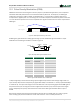
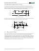
14 Accelerometer
The Nexys4 DDR includes an Analog Device ADXL362 accelerometer. The ADXL362 is a 3-axis MEMS accelerometer
that consumes less than 2μA at a 100Hz output data rate and 270nA when in motion triggered wake-up mode.
Unlike accelerometers that use power duty cycling to achieve low power consumption, the ADXL362 does not alias
input signals by under-sampling; it samples the full bandwidth of the sensor at all data rates. The ADXL362 always
provides 12-bit output resolution; 8-bit formatted data is also provided for more efficient single-byte transfers
when a lower resolution is sufficient. Measurement ranges of ±2 g, ±4 g, and ±8 g are available with a resolution of
1 mg/LSB on the ±2 g range. The FPGA can talk with the ADXL362 via SPI interface. While the ADXL362 is in
Measurement Mode, it continuously measures and stores acceleration data in the X-data, Y-data, and Z-data
registers. The interface between the FPGA and accelerometer can be seen in Figure 23.