
User Manual


Now, user can run the simulation and debug the design. The simulation allows user to test the
design without requiring lengthy synthesis process. Because the NetSUME-FPGA board has a
complex FPGA architecture, the bitstream generation process takes more than 45 minutes. The
simulation will be run in Vivado Simulator. To generate Ethernet packets, we used Scapy. The
details is at https://github.com/NetFPGA/NetFPGA-SUME-public/wiki/NetFPGA-SUME-
Simulations .
Once the user validate the design through simulation, they can generate the bitstream and
upload it on the board. This approach is suitable for digital designers who know Verilog or VHDL
and aim a high-performance system. For a software engineer or someone who want to parse
the incoming data and take action based on the packet header or payload, they should use P4.
P4 is a high level programming language that is used to describe packet processing logic and to
implement forwarding-plane of network elements. Users can describe the logic in P4 and use
Xilinx SDNet. The code can be compiled under Xilinx SDNet and the complied design can be
uploaded in NetSUME-FPGA. There is a simple switch example based for NetFGPA SUME in
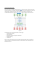
Xilinx SDNet (/opt/Xilinx/SDNet/<version_number>/data/p4include/sume_switch.p4). Figure 3
shows the switch architecture.
Figure 3