
Manual

PmodMIC3™ Reference Manual
Copyright Digilent, Inc. All rights reserved.
Other product and company names mentioned may be trademarks of their respective owners.
Page 2 of 3
2 Interfacing with the Pmod
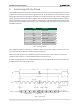
The PmodMIC3 communicates with the host board via the SPI protocol. The 12 bits of digital data are sent to the
system board in 16 clock cycles with the most significant bit first. For the ADC7476, each bit is shifted out on each
falling edge of the serial clock line after the chip select line is brought low with the first four bits as leading zeroes
and the remaining 12 bits representing the 12 bits of data. The datasheet for the ADC7476 recommends that for
faster microcontrollers or DSPs, the serial clock line is first brought to a high state before being brought low after
the fall of the chip select line to ensure that the first bit is valid. More information about this can be found in the
PmodMIC3 User Guide.
Table 1. Pinout table diagram.
The PmodMIC3 is capable of converting up to 1 MSa per second of 12-bit data, making it an ideal Pmod to use in
conjunction with the PmodI2S for an audio development application.
Any external power applied to the PmodMIC3 must be within 3V and 5.5V to ensure that the on-board chips
operate correctly; however, it is recommended that Pmod is operated at 3.3V.
A sample timing diagram taken from the ADCS7476 datasheet representing the data that will be received by the
system board from the Pmod is shown in FIg. 1.
Figure 1. Timing diagram.
Pin
Signal
Description
1
SS
Chip select
2
NC
Not connected
3
MISO
Master-in slave-out
4
SCK
Serial clock
5
GND
Power supply ground
6
VCC
Power supply (3.3V/5V)