
Data Sheet


Arty FPGA Board Reference Manual
Copyright Digilent, Inc. All rights reserved.
Other product and company names mentioned may be trademarks of their respective owners.
Page 16 of 18
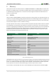
Pin Name
Shield Function
Arty Connection
IO0-IO13, IO26-IO41, A (IO42)
General purpose I/O pins
See Section titled “Shield Digital I/O”
SCL
I2C clock
See Section titled “Shield Digital I/O”
SDA
I2C data
See Section titled “Shield Digital I/O”
SCLK
SPI clock
See Section titled “Shield Digital I/O”
MOSI
SPI data out
See Section titled “Shield Digital I/O”
MISO
SPI data in
See Section titled “Shield Digital I/O”
SS
SPI slave select
See Section titled “Shield Digital I/O”
A0-A5
Single-ended analog input
See Section titled “Shield Digital I/O”
A6-A11
Differential analog input
See Section titled “Shield Digital I/O”
V_P, V_N
Dedicated differential analog
input
See Section titled “Shield Digital I/O”
XGND
XADC analog ground
Connected to net used to drive the XADC
ground reference on the FPGA (VREFN)
XVREF
XADC analog voltage
Connected to 1.25V, 25mA rail used to
drive the XADC voltage reference on the
FPGA (VREFP)
N/C
Not connected
Not connected
IOREF
Digital I/O voltage reference
Connected to the Arty 3.3V power rail (See
the “Power Supplies” section)
RST
Reset to shield
Connected to the red “RESET” button and
a digital I/O of the FPGA. When JP2 is
shorted, it is also connected to the DTR
signal of the FTDI USB-UART bridge.
3V3
3.3V power rail
Connected to the Arty 3.3V power rail (see
the “Power Supplies” section)
5V0
5.0V power rail
Connected to the Arty 5.0V power rail (see
the “Power Supplies” section)
GND, G
Ground
Connected to the ground plane of Arty
VIN
Power input
Connected in parallel with the external
power supply connector (J12). See the
“Power Supplies” section for information
on powering Arty from this pin.
Table 5. Shield connection table and functional description.
11.1 Shield Digital I/O
The pins connected directly to the FPGA can be used as general purpose inputs or outputs. These pins include the
I2C, SPI, and general purpose I/O pins. There are 200 Ohm series resistors between the FPGA and the digital I/O
pins to help provide protection against accidental short circuits. The absolute maximum and recommended
operating voltages for these pins are outlined in the table below.