
Data Sheet


Arty FPGA Board Reference Manual
Copyright Digilent, Inc. All rights reserved.
Other product and company names mentioned may be trademarks of their respective owners.
Page 17 of 18
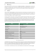
Table 6. Absolute maximum and recommended operating voltages.
For more information on the electrical characteristics of the pins connected to the FPGA, please see the Artix-7
datasheet from Xilinx.
11.2 Shield Analog I/O
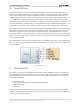
The pins labeled A0-A11 and V_P/V_N are used as analog inputs to the XADC module of the FPGA. The FPGA
expects that the inputs range from 0-1 V. On the pins labeled A0-A5 we use an external circuit to scale down the
input voltage from 3.3V. This circuit is shown in Figure 11.2.1. This circuit allows the XADC module to accurately
measure any voltage between 0V and 3.3V (relative to the Arty's GND) that is applied to any of these pins. If you
wish to use the pins labeled A0-A5 as Digital inputs or outputs, they are also connected directly to the FPGA before
the resistor divider circuit (also shown in Figure 11.2.1).
Figure 11.2.1. External circuit.
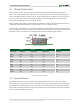
The pins labeled A6-A11 are connected directly to 3 pairs of analog capable pins on the FPGA via an anti-aliasing
filter. This circuit is shown in Figure 11.2.2. These pairs of pins can be used as differential analog inputs with a
voltage difference between 0-1V. The even numbers are connected to the positive pins of the pair and the odd
numbers are connected to the negative pins (so A6 and A7 form an analog input pair with A6 being positive and A7
being negative). Note that though the pads for the capacitor are present, they are not loaded for these pins. Since
the analog capable pins of the FPGA can also be used like normal digital FPGA pins, it is also possible to use these
pins for Digital I/O.
Absolute
Minimum Voltage
Recommended
Minimum
Operating Voltage
Recommended
Maximum Operating
Voltage
Absolute Maximum
Voltage
Powered
-0.4V
-0.2V
3.4V
3.75V
Unpowered
-0.4V
N/A
N/A
0.55V