
Data Sheet


Arty FPGA Board Reference Manual
Copyright Digilent, Inc. All rights reserved.
Other product and company names mentioned may be trademarks of their respective owners.
Page 9 of 18
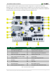
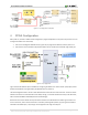
5 Memory
The Arty board contains two external memories: a 256MB DDR3L SDRAM and a 128Mb (16MB) non-volatile serial
flash device. The DDR3L module is connected to the FPGA using the industry standard interface. The serial flash is
on a dedicated quad-mode (x4) SPI bus. The connection and a pin assignment between the FPGA and external
memories are shown below.
5.1 DDR3L
The Arty includes one MT41K128M16JT-125 memory component, creating a single rank, 16-bit wide interface. It is
routed to a 1.35V-powered HR (High Range) FPGA bank with 50 ohm controlled single-ended trace impedance. 50
ohm internal terminations in the FPGA are used to match the trace characteristics. Similarly, on the memory side,
on-die terminations (ODT) are used for impedance matching.
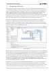
For proper operation of the memory, a memory controller and physical layer (PHY) interface needs to be included
in the FPGA design. The easiest way to accomplish this on the Arty is to use the Xilinx 7-series memory interface
solutions core generated by the MIG (Memory Interface Generator) Wizard. Depending on the tool used (ISE, EDK
or Vivado), the MIG Wizard can generate a native FIFO-style or an AXI4 interface to connect to user logic. This
workflow allows the customization of several DDR parameters optimized for the particular application. Table 2
below lists the MIG Wizard settings optimized for the Arty.
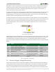
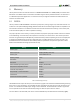
Table 3. DDR3L settings for the Arty.
The MIG Wizard will require the fixed pin-out of the memory signals to be entered and validated before generating
the IP core. For your convenience, an importable UCF file is provided on the Arty resource center to speed up this
process. It is included in the “MIG Project” design resource download. This download also includes a .prj file that
can be imported into the wizard to automatically configure it with the options found in Table 2.
For more details on the Xilinx MIG, refer to the 7 Series FPGAs Memory Interface Solutions User Guide (ug586).
Setting
Value
Memory type
DDR3 SDRAM
Max clock period
3000ps (667Mbps data rate)
Memory part
MT41K128M16XX-15E
Memory voltage
1.35V
Data width
16
Data mask
Enabled
Recommended input clock period
6000ps (166.667 MHz)
Output driver impedance control
RZQ/6
Controller chip select pin
Enabled
Rtt (nominal) – on-die termination
RZQ/6
Interval Vref
Enabled
Internal termination impedance
50omhs