Arty Z7 Reference Manual The Arty Z7 is a ready-to-use development platform designed around the Zynq-7000™ All Programmable System-on-Chip (AP SoC) from Xilinx. The Zynq-7000 architecture tightly integrates a dual-core, 650 MHz ARM Cortex-A9 processor with Xilinx 7-series Field Programmable Gate Array (FPGA) logic. This pairing grants the ability to surround a powerful processor with a unique set of software defined peripherals and controllers, tailored by you for the target application.
Features ZYNQ Processor o 650MHz dual-core Cortex-A9 processor o DDR3 memory controller with 8 DMA channels and 4 High Performance AXI3 Slave ports o High-bandwidth peripheral controllers: 1G Ethernet, USB 2.
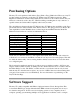
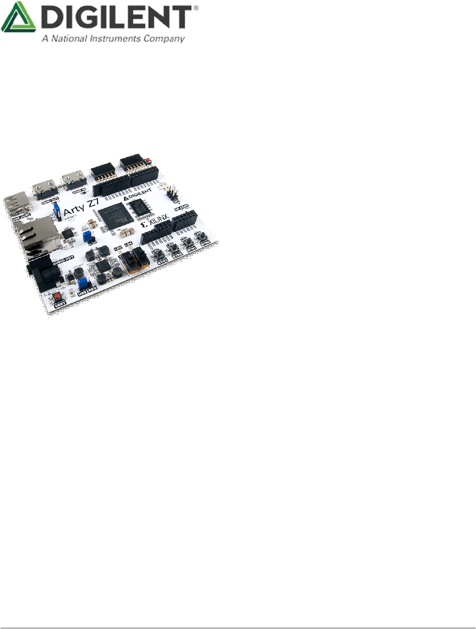
Purchasing Options The Arty Z7 can be purchased with either a Zynq-7010 or Zynq-7020 loaded. These two Arty Z7 product variants are referred to as the Arty Z7-7010 and Arty Z7-7020, respectively. When Digilent documentation describes functionality that is common to both of these variants, they are referred to collectively as the “Arty Z7”. When describing something that is only common to a specific variant, the variant will be explicitly called out by its name.
bare-metal program that controls some LEDs. It is also possible to treat the Zynq AP SoC as a standalone FPGA for those not interested in using the processor in their design. As of Vivado release 2015.4, the Logic Analyzer and High-level Synthesis features of Vivado are free to use for all WebPACK targets, which includes the Arty Z7. The Logic Analyzer assists with debugging logic, and the HLS tool allows you to compile C code directly into HDL.
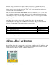
Similar to using an external power supply, a battery can be used to power the Arty Z7 by attaching it to the shield connector and setting jumper JP5 to “REG”. The positive terminal of the battery must be connected to the pin labeled “VIN” on J7, and the negative terminal must be connected to the pin labeled GND on J7. The on-board Texas Instruments TPS65400 PMU creates the required 3.3V, 1.8V, 1.5V, and 1.0V supplies from the main power input. Table 1.
The PL is nearly identical to a Xilinx 7-series Artix FPGA, except that it contains several dedicated ports and buses that tightly couple it to the PS. The PL also does not contain the same configuration hardware as a typical 7-series FPGA, and it must be configured either directly by the processor or via the JTAG port.
Reset 13 (N/C) 14 UART Input UART Output 15 MIO 501 1.
44 45 46 47 48 (N/C) 49 (N/C) 50 (N/C) 51 (N/C) 52 53 D2 D3 RESETN CD MDC MDIO Table 2.1. MIO Pinout 3 Zynq Configuration Unlike Xilinx FPGA devices, APSoC devices such as the Zynq-7020 are designed around the processor, which acts as a master to the programmable logic fabric and all other on-chip peripherals in the processing system. This causes the Zynq boot process to be more similar to that of a microcontroller than an FPGA.
Stage 1 During this stage, the FSBL first finishes configuring the PS components, such as the DDR memory controller. Then, if a bitstream is present in the Zynq Boot Image, it is read and used to configure the PL. Finally, the user application is loaded into memory from the Zynq Boot Image, and execution is handed off to it. Stage 2 The last stage is the execution of the user application that was loaded by the FSBL.
The three boot modes are described in the following sections. 3.1 microSD Boot Mode The Arty Z7 supports booting from a microSD card inserted into connector J9. The following procedure will allow you to boot the Zynq from microSD with a standard Zynq Boot Image created with the Xilinx tools: 1. 2. 3. 4. Format the microSD card with a FAT32 file system. Copy the Zynq Boot Image created with Xilinx SDK to the microSD card. Rename the Zynq Boot Image on the microSD card to BOOT.bin.
4 Quad SPI Flash The Arty Z7 features a Quad SPI serial NOR flash. The Spansion S25FL128S is used on this board. The Multi-I/O SPI Flash memory is used to provide non-volatile code and data storage. It can be used to initialize the PS subsystem as well as configure the PL subsystem. The relevant device attributes are: 16 MB x1, x2, and x4 support Bus speeds up to 104 MHz, supporting Zynq configuration rates @ 100 MHz. In Quad SPI mode, this translates to 400Mbs Powered from 3.
Both the memory chips and the PS DDR bank are powered from the 1.5V supply. The mid-point reference of 0.75V is created with a simple resistor divider and is available to the Zynq as external reference. For proper operation it is essential that the PS memory controller is configured properly. Settings range from the actual memory flavor to the board trace delays.
The FT2232HQ is also used as the controller for the Digilent USB-JTAG circuitry, but the USBUART and USB-JTAG functions behave entirely independent of one another. Programmers interested in using the UART functionality of the FT2232 within their design do not need to worry about the JTAG circuitry interfering with the UART data transfers, and vice-versa.
Figure 7.1. microSD slot signals Both low speed and high speed cards are supported, the maximum clock frequency being 50 MHz. A Class 4 card or better is recommended. Refer to section 3.1 for information on how to boot from an SD card. For more information, consult the Zynq Technical Reference manual. 8 USB Host The Arty Z7 implements one of the two available PS USB OTG interfaces on the Zynq device. A Microchip USB3320 USB 2.0 Transceiver Chip with an 8-bit ULPI interface is used as the PHY.
9 Ethernet PHY The Arty Z7 uses a Realtek RTL8211E-VL PHY to implement a 10/100/1000 Ethernet port for network connection. The PHY connects to MIO Bank 501 (1.8V) and interfaces to the Zynq7000 APSoC via RGMII for data and MDIO for management. The auxiliary interrupt (INTB) and reset (PHYRSTB) signals connect to MIO pins MIO10 and MIO9, respectively. Figure 9.1. Ethernet PHY signals After power-up the PHY starts with Auto Negotiation enabled, advertising 10/100/1000 link speeds and full duplex.
The Zynq incorporates two independent Gigabit Ethernet Controllers. They implement a 10/100/1000 half/full duplex Ethernet MAC. Of these two, GEM 0 can be mapped to the MIO pins where the PHY is connected. Since the MIO bank is powered from 1.8V, the RGMII interface uses 1.8V HSTL Class 1 drivers. For this I/O standard an external reference of 0.9V is provided in bank 501 (PS_MIO_VREF).
The 19-pin HDMI connectors include three differential data channels, one differential clock channel five GND connections, a one-wire Consumer Electronics Control (CEC) bus, a two-wire Display Data Channel (DDC) bus that is essentially an I2C bus, a Hot Plug Detect (HPD) signal, a 5V signal capable of delivering up to 50mA, and one reserved (RES) pin. All non-power signals are wired to the Zynq PL with the exception of RES.
the bus master being the source and the bus slave the sink. When a source detects high level on the HPD pin, it queries the sink over the DDC bus for video capabilities. It determines whether the sink is DVI or HDMI-capable and what resolutions are supported. Only afterwards will video transmission begin. Refer to VESA E-DDC specifications for more information.
Figure 11.1. Arty Z7 clocking. 12 Basic I/O The Arty Z7 board includes two tri-color LEDs, 2 switches, 4 push buttons, and 4 individual LEDs as shown in Figure 12.1. The push buttons and slide switches are connected to the Zynq PL via series resistors to prevent damage from inadvertent short circuits (a short circuit could occur if an FPGA pin assigned to a push button or slide switch was inadvertently defined as an output).
12.1 Tri-Color LEDs The Arty Z7 board contains two tri-color LEDs. Each tri-color LED has three input signals that drive the cathodes of three smaller internal LEDs: one red, one blue, and one green. Driving the signal corresponding to one of these colors high will illuminate the internal LED. The input signals are driven by the Zynq PL through a transistor, which inverts the signals. Therefore, to light up the tri-color LED, the corresponding signals need to be driven high.
The Audio shut-down signal (AUD_SD) is used to mute the audio output. It is connected to Zynq PL pin T17. To use the audio output, this signal must be driven to logic high. The frequency response of SK Butterworth Low-Pass Filter is shown in Figure 13.2. The AC analysis of the circuit is done using NI Multisim 12.0. Figure 13.2. Audio Output Frequency Response. 13.
The PWM signal must be integrated to define an analog voltage. The low-pass filter 3dB frequency should be an order of magnitude lower than the PWM frequency, so that signal energy at the PWM frequency is filtered from the signal. For example, if an audio signal must contain up to 5 KHz of frequency information, then the PWM frequency should be at least 50 KHz (and preferably even higher). In general, in terms of analog signal fidelity, the higher the PWM frequency, the better. Figure 13.1.
The SRST button also causes the CK_RST signal to toggle in order to trigger a reset on any attached shields. 15 Pmod Ports Pmod ports are 2×6, right-angle, 100-mil spaced female connectors that mate with standard 2×6 pin headers. Each 12-pin Pmod port provides two 3.3V VCC signals (pins 6 and 12), two Ground signals (pins 5 and 11), and eight logic signals, as shown in Figure 15.1.
Since the High-Speed Pmods have 0-ohm shunts instead of protection resistors, the operator must take precaution to ensure that they do not cause any shorts. 16 Arduino/chipKIT Shield Connector The Arty Z7 can be connected to standard Arduino and chipKIT shields to add extended functionality. Special care was taken while designing the Arty Z7 to make sure it is compatible with the majority of Arduino and chipKIT shields on the market.
Pin Name Shield Function General purpose I/O IO0-IO13 pins Arty Z7-7020 IO26-IO41, General purpose I/O A (IO42) pins I2C Clock SCL I2C Data SDA SPI Clock SCLK SPI Data out MOSI SPI Data in MISO SPI Slave Select SS Single-Ended A0-A5 Analog Input Differential Analog A6-A11 Input Dedicated V_P, V_N Differential Analog Input XADC Analog XGND Ground XADC Analog XVREF Voltage Reference Not Connected N/C Digital I/O Voltage IOREF reference RST Reset to Shield 3V3 3.3V Power Rail 5V0 5.
The pins connected directly to the Zynq PL can be used as general purpose inputs or outputs. These pins include the I2C, SPI, and general purpose I/O pins. There are 200 Ohm series resistors between the FPGA and the digital I/O pins to help provide protection against accidental short circuits (with the exception of the AN5-AN0 signals, which have no series resistors, and the AN6-AN12 signals, which have 100 Ohm series resistors).
Figure 16.2.1. Single-Ended Analog Inputs. The pins labeled A6-A11 are connected directly to 3 pairs of analog capable pins on the Zynq PL via an anti-aliasing filter. This circuit is shown in Figure 16.2.2. These pairs of pins can be used as differential analog inputs with a voltage difference between 0-1V.
The XADC core within the Zynq is a dual channel 12-bit analog-to-digital converter capable of operating at 1 MSPS. Either channel can be driven by any of the analog inputs connected to the shield pins. The XADC core is controlled and accessed from a user design via the Dynamic Reconfiguration Port (DRP). The DRP also provides access to voltage monitors that are present on each of the FPGA’s power rails, and a temperature sensor that is internal to the FPGA.