
User manual


Similar to using an external power supply, a battery can be used to power the Arty Z7 by
attaching it to the shield connector and setting jumper JP5 to “REG”. The positive terminal of the
battery must be connected to the pin labeled “VIN” on J7, and the negative terminal must be
connected to the pin labeled GND on J7.
The on-board Texas Instruments TPS65400 PMU creates the required 3.3V, 1.8V, 1.5V, and
1.0V supplies from the main power input. Table 1.1 provides additional information (typical
currents depend strongly on Zynq configuration and the values provided are typical of medium
size/speed designs).
The Arty Z7 does not have a power switch, so when a power source is connected and selected
with JP5 it will always be powered on. To reset the Zynq without disconnecting and
reconnecting the power supply, the red SRST button can be used. The power indicator LED
(LD13) is on when all the supply rails reach their nominal voltage.
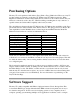
Supply Circuits Current (max/typical)
3.3V FPGA I/O, USB ports, Clocks, Ethernet, SD slot, Flash, HDMI 1.6A/0.1A to 1.5A
1.0V FPGA, Ethernet Core 2.6A/0.2A to 2.1A
1.5V DDR3 1.8A/0.1A to 1.2A
1.8V FPGA Auxiliary, Ethernet I/O, USB Controller 1.8A/0.1A to 0.6A
Table 1.1. Arty Z7 power supplies.
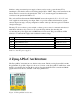
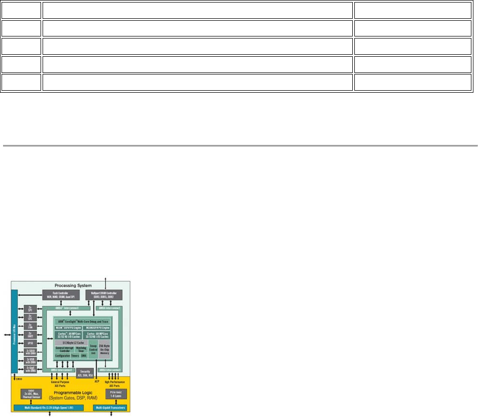
2 Zynq APSoC Architecture
The Zynq APSoC is divided into two distinct subsystems: The Processing System (PS) and the
Programmable Logic (PL). Figure 2.1 shows an overview of the Zynq APSoC architecture, with
the PS colored light green and the PL in yellow. Note that the PCIe Gen2 controller and Multi-
gigabit transceivers are not available on the Zynq-7020 device.
Figure 2.1 Zynq APSoC architecture