
User manual


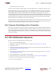
Table Of Contents
- Zynq-7000 All Programmable SoC
- Table of Contents
- Ch. 1: Introduction
- Ch. 2: Signals, Interfaces, and Pins
- Ch. 3: Application Processing Unit
- Ch. 4: System Addresses
- Ch. 5: Interconnect
- Ch. 6: Boot and Configuration
- Ch. 7: Interrupts
- Ch. 8: Timers
- Ch. 9: DMA Controller
- Introduction
- Functional Description
- DMA Transfers on the AXI Interconnect
- AXI Transaction Considerations
- DMA Manager
- Multi-channel Data FIFO (MFIFO)
- Memory-to-Memory Transfers
- PL Peripheral AXI Transactions
- PL Peripheral Request Interface
- PL Peripheral - Length Managed by PL Peripheral
- PL Peripheral - Length Managed by DMAC
- Events and Interrupts
- Aborts
- Security
- IP Configuration Options
- Programming Guide for DMA Controller
- Programming Guide for DMA Engine
- Programming Restrictions
- System Functions
- I/O Interface
- Ch. 10: DDR Memory Controller
- Introduction
- AXI Memory Port Interface (DDRI)
- DDR Core and Transaction Scheduler (DDRC)
- DDRC Arbitration
- Controller PHY (DDRP)
- Initialization and Calibration
- DDR Clock Initialization
- DDR IOB Impedance Calibration
- DDR IOB Configuration
- DDR Controller Register Programming
- DRAM Reset and Initialization
- DRAM Input Impedance (ODT) Calibration
- DRAM Output Impedance (RON) Calibration
- DRAM Training
- Write Data Eye Adjustment
- Alternatives to Automatic DRAM Training
- DRAM Write Latency Restriction
- Register Overview
- Error Correction Code (ECC)
- Programming Model
- Ch. 11: Static Memory Controller
- Ch. 12: Quad-SPI Flash Controller
- Ch. 13: SD/SDIO Controller
- Ch. 14: General Purpose I/O (GPIO)
- Ch. 15: USB Host, Device, and OTG Controller
- Introduction
- Functional Description
- Programming Overview and Reference
- Device Mode Control
- Device Endpoint Data Structures
- Device Endpoint Packet Operational Model
- Device Endpoint Descriptor Reference
- Programming Guide for Device Controller
- Programming Guide for Device Endpoint Data Structures
- Host Mode Data Structures
- EHCI Implementation
- Host Data Structures Reference
- Programming Guide for Host Controller
- OTG Description and Reference
- System Functions
- I/O Interfaces
- Ch. 16: Gigabit Ethernet Controller
- Ch. 17: SPI Controller
- Ch. 18: CAN Controller
- Ch. 19: UART Controller
- Ch. 20: I2C Controller
- Ch. 21: Programmable Logic Description
- Ch. 22: Programmable Logic Design Guide
- Ch. 23: Programmable Logic Test and Debug
- Ch. 24: Power Management
- Ch. 25: Clocks
- Ch. 26: Reset System
- Ch. 27: JTAG and DAP Subsystem
- Ch. 28: System Test and Debug
- Ch. 29: On-Chip Memory (OCM)
- Ch. 30: XADC Interface
- Ch. 31: PCI Express
- Ch. 32: Device Secure Boot
- Appx. A: Additional Resources
- Appx. B: Register Details
- Overview
- Acronyms
- Module Summary
- AXI_HP Interface (AFI) (axi_hp)
- CAN Controller (can)
- DDR Memory Controller (ddrc)
- CoreSight Cross Trigger Interface (cti)
- Performance Monitor Unit (cortexa9_pmu)
- CoreSight Program Trace Macrocell (ptm)
- Debug Access Port (dap)
- CoreSight Embedded Trace Buffer (etb)
- PL Fabric Trace Monitor (ftm)
- CoreSight Trace Funnel (funnel)
- CoreSight Intstrumentation Trace Macrocell (itm)
- CoreSight Trace Packet Output (tpiu)
- Device Configuration Interface (devcfg)
- DMA Controller (dmac)
- Gigabit Ethernet Controller (GEM)
- General Purpose I/O (gpio)
- Interconnect QoS (qos301)
- NIC301 Address Region Control (nic301_addr_region_ctrl_registers)
- I2C Controller (IIC)
- L2 Cache (L2Cpl310)
- Application Processing Unit (mpcore)
- On-Chip Memory (ocm)
- Quad-SPI Flash Controller (qspi)
- SD Controller (sdio)
- System Level Control Registers (slcr)
- Static Memory Controller (pl353)
- SPI Controller (SPI)
- System Watchdog Timer (swdt)
- Triple Timer Counter (ttc)
- UART Controller (UART)
- USB Controller (usb)

Zynq-7000 AP SoC Technical Reference Manual www.xilinx.com 104
UG585 (v1.11) September 27, 2016
Chapter 3: Application Processing Unit
Note: The transaction can optionally allocate into the L2 cache if the write parameters are set
accordingly.
ACP non-coherent write requests: An ACP write request is non-coherent when AWUSER[0] = 0 or
AWCACHE[1] = 0 alongside AWVALID. In this case, the SCU does not enforce coherency and the write
request is forwarded directly to one of the available SCU AXI master ports.
ACP Usage
The ACP provides a low latency path between the PS and the accelerators implemented in the PL
when compared with a legacy cache flushing and loading scheme. Steps that must take place in an
example of a PL-based accelerator are as follows:
1. The CPU prepares input data for the accelerator within its local cache space.
2. The CPU sends a message to the accelerator using one of the general purpose AXI master
interfaces to the PL.
3. The accelerator fetches the data through the ACP, processes the data, and returns the result
through the ACP.
4. The accelerator sets a flag by writing to a known location to indicate that the data processing is
complete. Status of this flag can be polled by the processor or could generate an interrupt.
Table 3-7 shows ACP read and write behavior based on current cache status. Clearly, access latency
is small when cache hits occur.
When compared to a tightly-coupled coprocessor, ACP access latencies are relatively long. Therefore,
ACP is not recommended for fine-grained instruction level acceleration. On the other hand, for
coarse-grain acceleration such as video frame-level processing, ACP does not have a clear advantage
over traditional memory-mapped PL acceleration because the transaction overhead is small relative
to the transaction time, and might potentially cause undesirable cache thrashing. ACP is therefore
optimal for medium-grain acceleration, such as block-level crypto accelerator and video
macro-block level processing.
Table 3-7: ACP Read and Write Behavior
Action Description
ACP read – I (invalid) SCU fetches data from external memory through one of two AXI master
interfaces. Data is forwarded to the ACP directly. It does not affect the CPU
L1 cache state.
ACP read – M (modified) SCU fetches data from L1 cache with M status. It does not affect the L1
cache state.
ACP read – S (shared) SCU fetches data from any L1 cache with S status. It does not affect the L1
cache state.
ACP read – E (exclusive) SCU fetches data from the L1 cache with E status. It does not affect the L1
cache state.
ACP write – I (invalid) Data is written to external memory through one of two AXI master
interfaces. It does not affect the CPU L1 cache state.
ACP write – M (modified) Data in L1 cache with M status is flushed out to external memory first.
After that, ACP data is written into external memory interface. L1 cache
previously with M status is changed to I status. If the SCU overwrites the
entire cache line, L1 cache flush is skipped.