
User manual


Table Of Contents
- Zynq-7000 All Programmable SoC
- Table of Contents
- Ch. 1: Introduction
- Ch. 2: Signals, Interfaces, and Pins
- Ch. 3: Application Processing Unit
- Ch. 4: System Addresses
- Ch. 5: Interconnect
- Ch. 6: Boot and Configuration
- Ch. 7: Interrupts
- Ch. 8: Timers
- Ch. 9: DMA Controller
- Introduction
- Functional Description
- DMA Transfers on the AXI Interconnect
- AXI Transaction Considerations
- DMA Manager
- Multi-channel Data FIFO (MFIFO)
- Memory-to-Memory Transfers
- PL Peripheral AXI Transactions
- PL Peripheral Request Interface
- PL Peripheral - Length Managed by PL Peripheral
- PL Peripheral - Length Managed by DMAC
- Events and Interrupts
- Aborts
- Security
- IP Configuration Options
- Programming Guide for DMA Controller
- Programming Guide for DMA Engine
- Programming Restrictions
- System Functions
- I/O Interface
- Ch. 10: DDR Memory Controller
- Introduction
- AXI Memory Port Interface (DDRI)
- DDR Core and Transaction Scheduler (DDRC)
- DDRC Arbitration
- Controller PHY (DDRP)
- Initialization and Calibration
- DDR Clock Initialization
- DDR IOB Impedance Calibration
- DDR IOB Configuration
- DDR Controller Register Programming
- DRAM Reset and Initialization
- DRAM Input Impedance (ODT) Calibration
- DRAM Output Impedance (RON) Calibration
- DRAM Training
- Write Data Eye Adjustment
- Alternatives to Automatic DRAM Training
- DRAM Write Latency Restriction
- Register Overview
- Error Correction Code (ECC)
- Programming Model
- Ch. 11: Static Memory Controller
- Ch. 12: Quad-SPI Flash Controller
- Ch. 13: SD/SDIO Controller
- Ch. 14: General Purpose I/O (GPIO)
- Ch. 15: USB Host, Device, and OTG Controller
- Introduction
- Functional Description
- Programming Overview and Reference
- Device Mode Control
- Device Endpoint Data Structures
- Device Endpoint Packet Operational Model
- Device Endpoint Descriptor Reference
- Programming Guide for Device Controller
- Programming Guide for Device Endpoint Data Structures
- Host Mode Data Structures
- EHCI Implementation
- Host Data Structures Reference
- Programming Guide for Host Controller
- OTG Description and Reference
- System Functions
- I/O Interfaces
- Ch. 16: Gigabit Ethernet Controller
- Ch. 17: SPI Controller
- Ch. 18: CAN Controller
- Ch. 19: UART Controller
- Ch. 20: I2C Controller
- Ch. 21: Programmable Logic Description
- Ch. 22: Programmable Logic Design Guide
- Ch. 23: Programmable Logic Test and Debug
- Ch. 24: Power Management
- Ch. 25: Clocks
- Ch. 26: Reset System
- Ch. 27: JTAG and DAP Subsystem
- Ch. 28: System Test and Debug
- Ch. 29: On-Chip Memory (OCM)
- Ch. 30: XADC Interface
- Ch. 31: PCI Express
- Ch. 32: Device Secure Boot
- Appx. A: Additional Resources
- Appx. B: Register Details
- Overview
- Acronyms
- Module Summary
- AXI_HP Interface (AFI) (axi_hp)
- CAN Controller (can)
- DDR Memory Controller (ddrc)
- CoreSight Cross Trigger Interface (cti)
- Performance Monitor Unit (cortexa9_pmu)
- CoreSight Program Trace Macrocell (ptm)
- Debug Access Port (dap)
- CoreSight Embedded Trace Buffer (etb)
- PL Fabric Trace Monitor (ftm)
- CoreSight Trace Funnel (funnel)
- CoreSight Intstrumentation Trace Macrocell (itm)
- CoreSight Trace Packet Output (tpiu)
- Device Configuration Interface (devcfg)
- DMA Controller (dmac)
- Gigabit Ethernet Controller (GEM)
- General Purpose I/O (gpio)
- Interconnect QoS (qos301)
- NIC301 Address Region Control (nic301_addr_region_ctrl_registers)
- I2C Controller (IIC)
- L2 Cache (L2Cpl310)
- Application Processing Unit (mpcore)
- On-Chip Memory (ocm)
- Quad-SPI Flash Controller (qspi)
- SD Controller (sdio)
- System Level Control Registers (slcr)
- Static Memory Controller (pl353)
- SPI Controller (SPI)
- System Watchdog Timer (swdt)
- Triple Timer Counter (ttc)
- UART Controller (UART)
- USB Controller (usb)
Zynq-7000 AP SoC Technical Reference Manual www.xilinx.com 108
UG585 (v1.11) September 27, 2016
Chapter 3: Application Processing Unit
Note: Unlike the POR or system resets, when the user applies a software reset to a single processor,
the user must stop the associated clock, de-assert the reset, and then restart the clock. During a
system or POR reset, hardware automatically takes care of this. Therefore, a CPU cannot run the code
that applies the software reset to itself. This reset needs to be applied by the other CPU or through
JTAG or PL. Assuming the user wants to reset CPU0, the user must to set the following fields in the
slcr.A9_CPU_RST_CTRL (address 0x000244) register in the order listed:
1. A9_RST0 = 1 to assert reset to CPU0
2. A9_CLKSTOP0 = 1 to stop clock to CPU0
3. A9_RST0 = 0 to release reset to CPU0
4. A9_CLKSTOP0 = 0 to restart clock to CPU0
3.7.2 APU State After Reset
Table 3-9 summarizes the state of the APU after the reset. For a CPU, including its L1 caches and
MMU, this reset is a CPU reset that can be triggered through all resets. The reset to the SCU and the
L2 cache can occur as a result of a system software reset, external system reset, debug system reset,
and watchdog timer resets.
3.8 Power Considerations
The system-level power consideration are described in Chapter 24, Power Management. System
Modules, page 673 includes additional information on the APU.
3.8.1 Introduction
The APU incorporates many features to improve its dynamic power efficiency:
• Either of the CPUs can be put in the standby mode and started up when a event or interrupt is
detected.
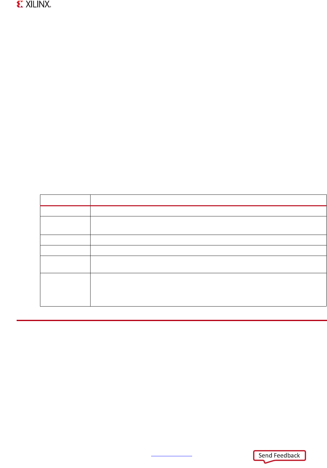
Table 3-9: APU State after Reset
Function State after Reset
CPU1 Kept in a WFE state while executing code located at address 0xFFFFFE00 to 0xFFFFFFF0
L1 Caches
Validation
Disabled
Unknown (requires invalidation prior to usage)
MMUs Disabled
SCU Disabled
Address Filtering Upper and lower 1M addresses within the 4G address space are mapped to OCM and the
rest of the addresses are routed to the L2
L2 Cache
L2 wait states
Validation
Disabled
Tag RAM and Data RAM wait states are both 7-7-7 for setup latency, write access latency,
and read access latency
Unknown (requires invalidation prior to usage)