
User manual


Table Of Contents
- Zynq-7000 All Programmable SoC
- Table of Contents
- Ch. 1: Introduction
- Ch. 2: Signals, Interfaces, and Pins
- Ch. 3: Application Processing Unit
- Ch. 4: System Addresses
- Ch. 5: Interconnect
- Ch. 6: Boot and Configuration
- Ch. 7: Interrupts
- Ch. 8: Timers
- Ch. 9: DMA Controller
- Introduction
- Functional Description
- DMA Transfers on the AXI Interconnect
- AXI Transaction Considerations
- DMA Manager
- Multi-channel Data FIFO (MFIFO)
- Memory-to-Memory Transfers
- PL Peripheral AXI Transactions
- PL Peripheral Request Interface
- PL Peripheral - Length Managed by PL Peripheral
- PL Peripheral - Length Managed by DMAC
- Events and Interrupts
- Aborts
- Security
- IP Configuration Options
- Programming Guide for DMA Controller
- Programming Guide for DMA Engine
- Programming Restrictions
- System Functions
- I/O Interface
- Ch. 10: DDR Memory Controller
- Introduction
- AXI Memory Port Interface (DDRI)
- DDR Core and Transaction Scheduler (DDRC)
- DDRC Arbitration
- Controller PHY (DDRP)
- Initialization and Calibration
- DDR Clock Initialization
- DDR IOB Impedance Calibration
- DDR IOB Configuration
- DDR Controller Register Programming
- DRAM Reset and Initialization
- DRAM Input Impedance (ODT) Calibration
- DRAM Output Impedance (RON) Calibration
- DRAM Training
- Write Data Eye Adjustment
- Alternatives to Automatic DRAM Training
- DRAM Write Latency Restriction
- Register Overview
- Error Correction Code (ECC)
- Programming Model
- Ch. 11: Static Memory Controller
- Ch. 12: Quad-SPI Flash Controller
- Ch. 13: SD/SDIO Controller
- Ch. 14: General Purpose I/O (GPIO)
- Ch. 15: USB Host, Device, and OTG Controller
- Introduction
- Functional Description
- Programming Overview and Reference
- Device Mode Control
- Device Endpoint Data Structures
- Device Endpoint Packet Operational Model
- Device Endpoint Descriptor Reference
- Programming Guide for Device Controller
- Programming Guide for Device Endpoint Data Structures
- Host Mode Data Structures
- EHCI Implementation
- Host Data Structures Reference
- Programming Guide for Host Controller
- OTG Description and Reference
- System Functions
- I/O Interfaces
- Ch. 16: Gigabit Ethernet Controller
- Ch. 17: SPI Controller
- Ch. 18: CAN Controller
- Ch. 19: UART Controller
- Ch. 20: I2C Controller
- Ch. 21: Programmable Logic Description
- Ch. 22: Programmable Logic Design Guide
- Ch. 23: Programmable Logic Test and Debug
- Ch. 24: Power Management
- Ch. 25: Clocks
- Ch. 26: Reset System
- Ch. 27: JTAG and DAP Subsystem
- Ch. 28: System Test and Debug
- Ch. 29: On-Chip Memory (OCM)
- Ch. 30: XADC Interface
- Ch. 31: PCI Express
- Ch. 32: Device Secure Boot
- Appx. A: Additional Resources
- Appx. B: Register Details
- Overview
- Acronyms
- Module Summary
- AXI_HP Interface (AFI) (axi_hp)
- CAN Controller (can)
- DDR Memory Controller (ddrc)
- CoreSight Cross Trigger Interface (cti)
- Performance Monitor Unit (cortexa9_pmu)
- CoreSight Program Trace Macrocell (ptm)
- Debug Access Port (dap)
- CoreSight Embedded Trace Buffer (etb)
- PL Fabric Trace Monitor (ftm)
- CoreSight Trace Funnel (funnel)
- CoreSight Intstrumentation Trace Macrocell (itm)
- CoreSight Trace Packet Output (tpiu)
- Device Configuration Interface (devcfg)
- DMA Controller (dmac)
- Gigabit Ethernet Controller (GEM)
- General Purpose I/O (gpio)
- Interconnect QoS (qos301)
- NIC301 Address Region Control (nic301_addr_region_ctrl_registers)
- I2C Controller (IIC)
- L2 Cache (L2Cpl310)
- Application Processing Unit (mpcore)
- On-Chip Memory (ocm)
- Quad-SPI Flash Controller (qspi)
- SD Controller (sdio)
- System Level Control Registers (slcr)
- Static Memory Controller (pl353)
- SPI Controller (SPI)
- System Watchdog Timer (swdt)
- Triple Timer Counter (ttc)
- UART Controller (UART)
- USB Controller (usb)
Zynq-7000 AP SoC Technical Reference Manual www.xilinx.com 113
UG585 (v1.11) September 27, 2016
Chapter 4: System Addresses
PL AXI Interface Note
There are two general purpose interconnect ports that go to the PL, M_AXI_GP{1,0}. Each port is
addressable by masters in the PS and each port occupies 1 GB of system address space in the ranges
specified in Table 4-1. The M_AXI_GP addresses are directly from the PS; they are not remapped on
their way to the PL. The addresses outside of these ranges are not presented to the PL.
Execute-In-Place Capable Devices
The following devices are execute-in-place capable:
• DDR
•OCM
•SMC SRAM/NOR
• Quad-SPI (linear addressing mode)
• M_AXI_GP{1, 0} (PL block RAM or external memory with a suitable PL slave controller)
Notes:
1. The other bus masters include the S_AXI_GP interfaces, Device configuration interface (DevC), DAP controller, DMA
controller and the various controllers with local DMA units (Ethernet, USB and SDIO).
2. The OCM is divided into four 64 KB sections. Each section is mapped independently to either the low or high
addresses ranges, but not both at the same time. In addition, the SCU can filter addresses destined for the OCM
low address range to the DDR DRAM controller instead. A detailed discussion of the OCM is explained in
Chapter 29, On-Chip Memory (OCM).
3. For each 64 KB section mapped to the high OCM address range via slcr.OCM_CFG[RAM_HI] which is not also part
of the SCU address filtering range will be aliased for CPU and ACP masters at a range of (0x000C_0000 to
0x000F_FFFF). See Chapter 29, On-Chip Memory (OCM) for more information.
4. When a single device is used, it must be connected to QSPI 0. In this case, the address map starts at FC00_0000
and goes to a maximum of FCFF_FFFF (16 MBs). When two devices are used, both devices must be the same
capacity. The address map for two devices depends on the size of the devices and their connection configuration.
For the shared 4-bit stacked I/O bus, the QSPI 0 device starts at FC00_0000 and goes to a maximum of
FCFF_FFFF (16 MBs). The QSPI 1 device starts at FD00_0000 and goes to a maximum of FDFF_FFFF (another 16
MBs). If the first device is less than 16 MBs in size, then there will be a memory space hole between the two
devices. For the 8-bit dual parallel mode (8-bit bus), the memory map is continuous from FC00_0000 to a
maximum of FDFF_FFFF (32 MBs).
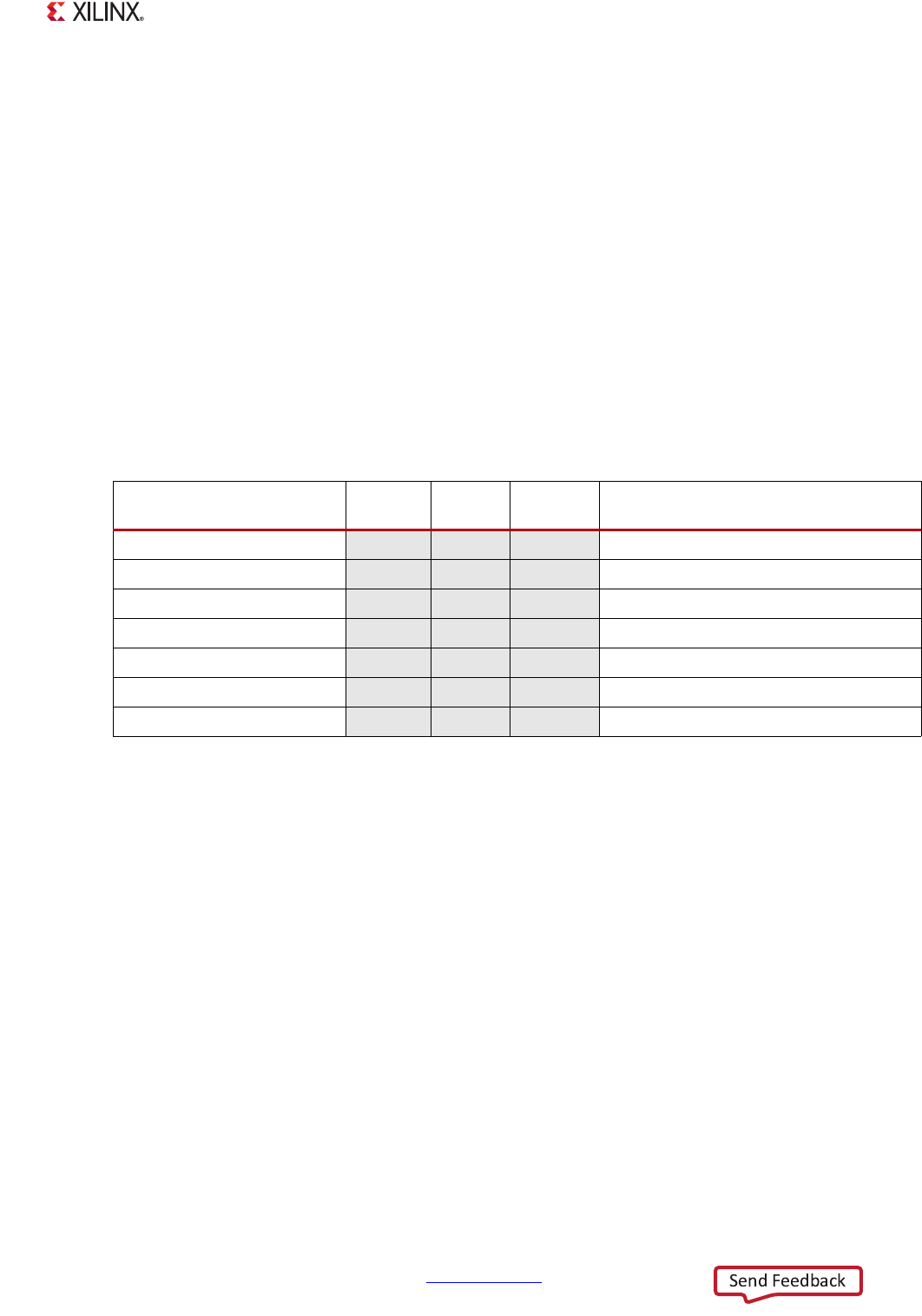
Table 4-2: System-Level Address Map (Reserved Addresses)
Address Range
CPUs and
ACP
AXI_HP
Other Bus
Masters
(1)
Notes
C000_0000 to DFFF_FFFF Reserved
E030_0000 to E0FF_FFFF
Reserved
E600_0000 to F7FF_FFFF
Reserved
F800_0C00 to F800_0FFF
Reserved
F881_0000 to F889_0FFF
Reserved
F8F0_3000 to FBFF_FFFF
Reserved
FE00_0000 to FFFB_FFFF
Reserved