
User manual


Table Of Contents
- Zynq-7000 All Programmable SoC
- Table of Contents
- Ch. 1: Introduction
- Ch. 2: Signals, Interfaces, and Pins
- Ch. 3: Application Processing Unit
- Ch. 4: System Addresses
- Ch. 5: Interconnect
- Ch. 6: Boot and Configuration
- Ch. 7: Interrupts
- Ch. 8: Timers
- Ch. 9: DMA Controller
- Introduction
- Functional Description
- DMA Transfers on the AXI Interconnect
- AXI Transaction Considerations
- DMA Manager
- Multi-channel Data FIFO (MFIFO)
- Memory-to-Memory Transfers
- PL Peripheral AXI Transactions
- PL Peripheral Request Interface
- PL Peripheral - Length Managed by PL Peripheral
- PL Peripheral - Length Managed by DMAC
- Events and Interrupts
- Aborts
- Security
- IP Configuration Options
- Programming Guide for DMA Controller
- Programming Guide for DMA Engine
- Programming Restrictions
- System Functions
- I/O Interface
- Ch. 10: DDR Memory Controller
- Introduction
- AXI Memory Port Interface (DDRI)
- DDR Core and Transaction Scheduler (DDRC)
- DDRC Arbitration
- Controller PHY (DDRP)
- Initialization and Calibration
- DDR Clock Initialization
- DDR IOB Impedance Calibration
- DDR IOB Configuration
- DDR Controller Register Programming
- DRAM Reset and Initialization
- DRAM Input Impedance (ODT) Calibration
- DRAM Output Impedance (RON) Calibration
- DRAM Training
- Write Data Eye Adjustment
- Alternatives to Automatic DRAM Training
- DRAM Write Latency Restriction
- Register Overview
- Error Correction Code (ECC)
- Programming Model
- Ch. 11: Static Memory Controller
- Ch. 12: Quad-SPI Flash Controller
- Ch. 13: SD/SDIO Controller
- Ch. 14: General Purpose I/O (GPIO)
- Ch. 15: USB Host, Device, and OTG Controller
- Introduction
- Functional Description
- Programming Overview and Reference
- Device Mode Control
- Device Endpoint Data Structures
- Device Endpoint Packet Operational Model
- Device Endpoint Descriptor Reference
- Programming Guide for Device Controller
- Programming Guide for Device Endpoint Data Structures
- Host Mode Data Structures
- EHCI Implementation
- Host Data Structures Reference
- Programming Guide for Host Controller
- OTG Description and Reference
- System Functions
- I/O Interfaces
- Ch. 16: Gigabit Ethernet Controller
- Ch. 17: SPI Controller
- Ch. 18: CAN Controller
- Ch. 19: UART Controller
- Ch. 20: I2C Controller
- Ch. 21: Programmable Logic Description
- Ch. 22: Programmable Logic Design Guide
- Ch. 23: Programmable Logic Test and Debug
- Ch. 24: Power Management
- Ch. 25: Clocks
- Ch. 26: Reset System
- Ch. 27: JTAG and DAP Subsystem
- Ch. 28: System Test and Debug
- Ch. 29: On-Chip Memory (OCM)
- Ch. 30: XADC Interface
- Ch. 31: PCI Express
- Ch. 32: Device Secure Boot
- Appx. A: Additional Resources
- Appx. B: Register Details
- Overview
- Acronyms
- Module Summary
- AXI_HP Interface (AFI) (axi_hp)
- CAN Controller (can)
- DDR Memory Controller (ddrc)
- CoreSight Cross Trigger Interface (cti)
- Performance Monitor Unit (cortexa9_pmu)
- CoreSight Program Trace Macrocell (ptm)
- Debug Access Port (dap)
- CoreSight Embedded Trace Buffer (etb)
- PL Fabric Trace Monitor (ftm)
- CoreSight Trace Funnel (funnel)
- CoreSight Intstrumentation Trace Macrocell (itm)
- CoreSight Trace Packet Output (tpiu)
- Device Configuration Interface (devcfg)
- DMA Controller (dmac)
- Gigabit Ethernet Controller (GEM)
- General Purpose I/O (gpio)
- Interconnect QoS (qos301)
- NIC301 Address Region Control (nic301_addr_region_ctrl_registers)
- I2C Controller (IIC)
- L2 Cache (L2Cpl310)
- Application Processing Unit (mpcore)
- On-Chip Memory (ocm)
- Quad-SPI Flash Controller (qspi)
- SD Controller (sdio)
- System Level Control Registers (slcr)
- Static Memory Controller (pl353)
- SPI Controller (SPI)
- System Watchdog Timer (swdt)
- Triple Timer Counter (ttc)
- UART Controller (UART)
- USB Controller (usb)
Zynq-7000 AP SoC Technical Reference Manual www.xilinx.com 114
UG585 (v1.11) September 27, 2016
Chapter 4: System Addresses
4.2 System Bus Masters
The CPUs and AXI_ACP see the same memory map, except the CPUs have a private bus to access their
private timer, interrupt controller, and shared L2 cache / SCU registers. The AXI_HP interfaces provide
high bandwidth to the DDR DRAM and OCM memory. The other system bus masters include:
• DMA controller, see Chapter 9, DMA Controller
• Device configuration interface (DevC), see Chapter 6, Boot and Configuration
• Debug access port (DAP), see Chapter 28, System Test and Debug
• PL bus master controllers attached to AXI general purpose ports (S_AXI_GP[1:0]), see Chapter 5,
Interconnect and Chapter 21, Programmable Logic Description
• AHB bus master ports with local DMA units (Ethernet, USB, and SDIO)
4.3 SLCR Registers
The System-Level Control registers (SLCR) consist of various registers that are used to control the PS
behavior. These registers are accessible via the central interconnect using load and store instructions.
The detailed descriptions for each register can be found in Appendix B, Register Details. A summary
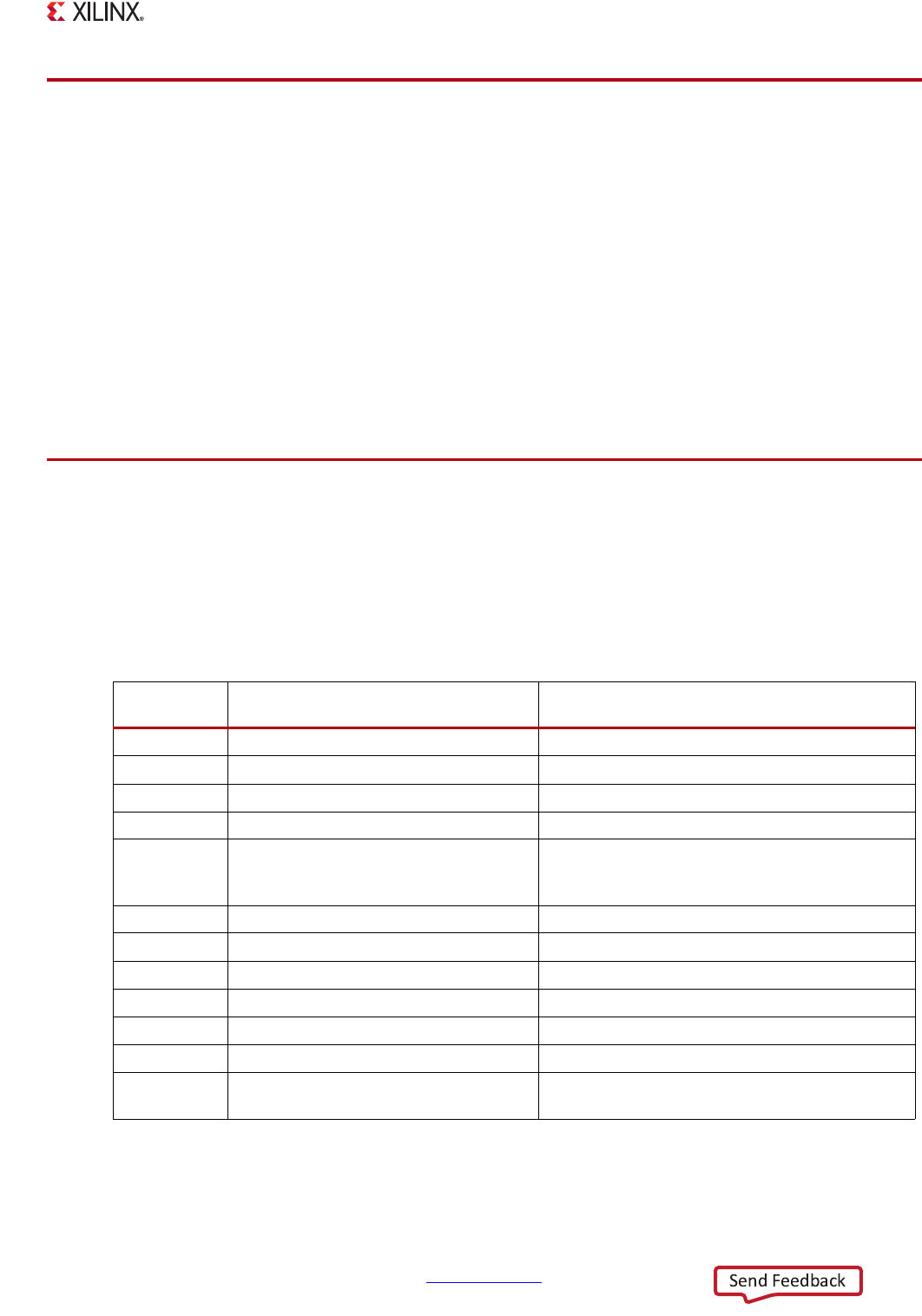
of the SLCR registers with their base addresses is shown in Table 4-3.
Table 4-3: SLCR Register Map
Register Base
Address
Description Reference
F800_0000 SLCR write protection lock and security
F800_0100 Clock control and status See Chapter 25, Clocks
F800_0200 Reset control and status See Chapter 26, Reset System
F800_0300 APU control See Chapter 3, Application Processing Unit
F800_0400 TrustZone control
See UG1019, Programming ARM TrustZone
Architecture on the Xilinx Zynq-7000 All
Programmable SoC
F800_0500 CoreSight SoC debug control See Chapter 28, System Test and Debug
F800_0600 DDR DRAM controller See Chapter 10, DDR Memory Controller
F800_0700 MIO pin configuration See Chapter 2, Signals, Interfaces, and Pins
F800_0800 MIO parallel access See Chapter 2, Signals, Interfaces, and Pins
F800_0900 Miscellaneous control See Chapter 29, On-Chip Memory (OCM)
F800_0A00 On-chip memory (OCM) control See Chapter 29, On-Chip Memory (OCM)
F800_0B00
I/O buffers for MIO pins (GPIOB) and
DDR pins (DDRIOB)
See Chapter 2, Signals, Interfaces, and Pins