
User manual


Table Of Contents
- Zynq-7000 All Programmable SoC
- Table of Contents
- Ch. 1: Introduction
- Ch. 2: Signals, Interfaces, and Pins
- Ch. 3: Application Processing Unit
- Ch. 4: System Addresses
- Ch. 5: Interconnect
- Ch. 6: Boot and Configuration
- Ch. 7: Interrupts
- Ch. 8: Timers
- Ch. 9: DMA Controller
- Introduction
- Functional Description
- DMA Transfers on the AXI Interconnect
- AXI Transaction Considerations
- DMA Manager
- Multi-channel Data FIFO (MFIFO)
- Memory-to-Memory Transfers
- PL Peripheral AXI Transactions
- PL Peripheral Request Interface
- PL Peripheral - Length Managed by PL Peripheral
- PL Peripheral - Length Managed by DMAC
- Events and Interrupts
- Aborts
- Security
- IP Configuration Options
- Programming Guide for DMA Controller
- Programming Guide for DMA Engine
- Programming Restrictions
- System Functions
- I/O Interface
- Ch. 10: DDR Memory Controller
- Introduction
- AXI Memory Port Interface (DDRI)
- DDR Core and Transaction Scheduler (DDRC)
- DDRC Arbitration
- Controller PHY (DDRP)
- Initialization and Calibration
- DDR Clock Initialization
- DDR IOB Impedance Calibration
- DDR IOB Configuration
- DDR Controller Register Programming
- DRAM Reset and Initialization
- DRAM Input Impedance (ODT) Calibration
- DRAM Output Impedance (RON) Calibration
- DRAM Training
- Write Data Eye Adjustment
- Alternatives to Automatic DRAM Training
- DRAM Write Latency Restriction
- Register Overview
- Error Correction Code (ECC)
- Programming Model
- Ch. 11: Static Memory Controller
- Ch. 12: Quad-SPI Flash Controller
- Ch. 13: SD/SDIO Controller
- Ch. 14: General Purpose I/O (GPIO)
- Ch. 15: USB Host, Device, and OTG Controller
- Introduction
- Functional Description
- Programming Overview and Reference
- Device Mode Control
- Device Endpoint Data Structures
- Device Endpoint Packet Operational Model
- Device Endpoint Descriptor Reference
- Programming Guide for Device Controller
- Programming Guide for Device Endpoint Data Structures
- Host Mode Data Structures
- EHCI Implementation
- Host Data Structures Reference
- Programming Guide for Host Controller
- OTG Description and Reference
- System Functions
- I/O Interfaces
- Ch. 16: Gigabit Ethernet Controller
- Ch. 17: SPI Controller
- Ch. 18: CAN Controller
- Ch. 19: UART Controller
- Ch. 20: I2C Controller
- Ch. 21: Programmable Logic Description
- Ch. 22: Programmable Logic Design Guide
- Ch. 23: Programmable Logic Test and Debug
- Ch. 24: Power Management
- Ch. 25: Clocks
- Ch. 26: Reset System
- Ch. 27: JTAG and DAP Subsystem
- Ch. 28: System Test and Debug
- Ch. 29: On-Chip Memory (OCM)
- Ch. 30: XADC Interface
- Ch. 31: PCI Express
- Ch. 32: Device Secure Boot
- Appx. A: Additional Resources
- Appx. B: Register Details
- Overview
- Acronyms
- Module Summary
- AXI_HP Interface (AFI) (axi_hp)
- CAN Controller (can)
- DDR Memory Controller (ddrc)
- CoreSight Cross Trigger Interface (cti)
- Performance Monitor Unit (cortexa9_pmu)
- CoreSight Program Trace Macrocell (ptm)
- Debug Access Port (dap)
- CoreSight Embedded Trace Buffer (etb)
- PL Fabric Trace Monitor (ftm)
- CoreSight Trace Funnel (funnel)
- CoreSight Intstrumentation Trace Macrocell (itm)
- CoreSight Trace Packet Output (tpiu)
- Device Configuration Interface (devcfg)
- DMA Controller (dmac)
- Gigabit Ethernet Controller (GEM)
- General Purpose I/O (gpio)
- Interconnect QoS (qos301)
- NIC301 Address Region Control (nic301_addr_region_ctrl_registers)
- I2C Controller (IIC)
- L2 Cache (L2Cpl310)
- Application Processing Unit (mpcore)
- On-Chip Memory (ocm)
- Quad-SPI Flash Controller (qspi)
- SD Controller (sdio)
- System Level Control Registers (slcr)
- Static Memory Controller (pl353)
- SPI Controller (SPI)
- System Watchdog Timer (swdt)
- Triple Timer Counter (ttc)
- UART Controller (UART)
- USB Controller (usb)
Zynq-7000 AP SoC Technical Reference Manual www.xilinx.com 1151
UG585 (v1.11) September 27, 2016
Appendix B: Register Details
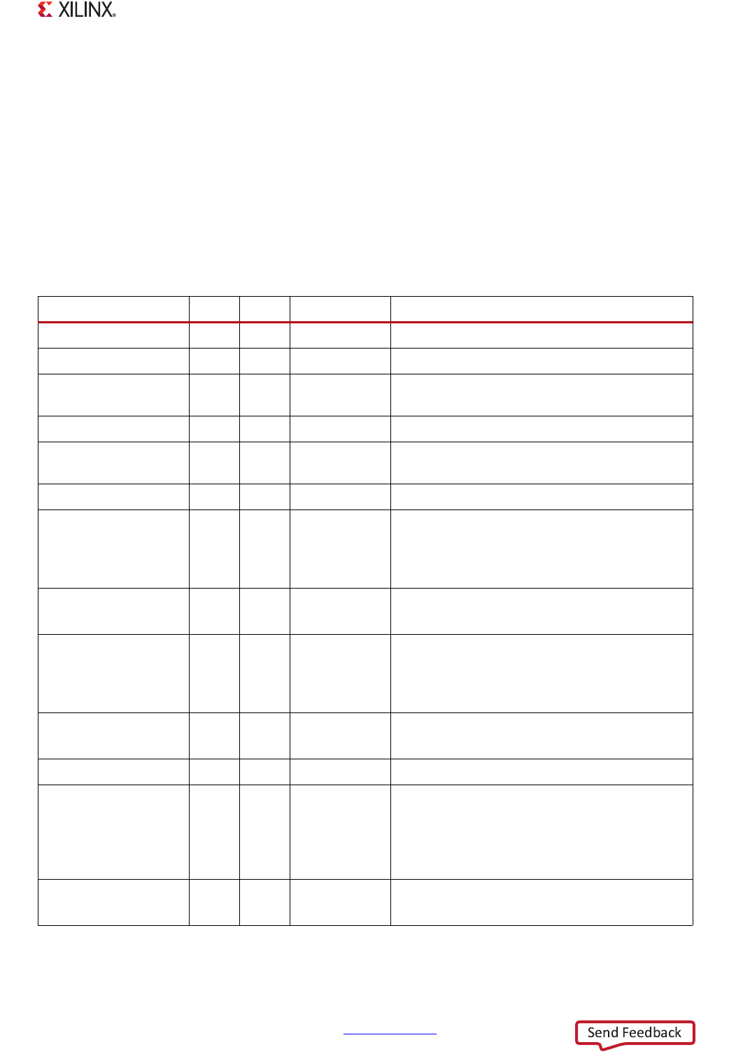
Register INT_STS Details
Access Type mixed
Reset Value 0x00000000
Description Interrupt Status Register : This register contains interrupt status flags.
All register bits are clear on write by writing 1s to those bits, however the register bits
will only be cleared if the condition that sets the interrupt flag is no longer true.
Note that individual status bits will be set if the corresponding condition is satisfied
regardless of whether the interrupt mask bit in 0x010 is set.
However, external interrupt will only be generated if an interrupt status flag is set
and the corresponding mask bit is not set
Field Name Bits Type Reset Value Description
PSS_GTS_USR_B_INT 31 wtc 0x0 Tri-state PL IO during HIZ, both edges
PSS_FST_CFG_B_INT 30 wtc 0x0 First configuration done, both edges
PSS_GPWRDWN_B_I
NT
29 wtc 0x0 Global power down, both edges
PSS_GTS_CFG_B_INT 28 wtc 0x0 Tri-state PL IO during configuration, both edges
PSS_CFG_RESET_B_I
NT
27 wtc 0x0 PL configuration reset, both edges
reserved 26:24 rw 0x0 Reserved
AXI_WTO_INT
(IXR_AXI_WTO)
23 wtc 0x0 AXI write address, data or response time out.
AXI write is taking longer than expected (> 6144
cpu_1x clock cycles), this can be an indication of
starvation
AXI_WERR_INT
(IXR_AXI_WERR)
22 wtc 0x0 AXI write response error
AXI_RTO_INT
(IXR_AXI_RTO)
21 wtc 0x0 AXI read address or response time out.
AXI read is taking longer than expected (> 2048
cpu_1x clock cycles), this can be an indication of
starvation
AXI_RERR_INT
(IXR_AXI_RERR)
20 wtc 0x0 AXI read response error
reserved 19 rw 0x0 Reserved
RX_FIFO_OV_INT
(IXR_RX_FIFO_OV)
18 wtc 0x0 This bit is used to indicate that RX FIFO
overflows. Incoming read data from PCAP will be
dropped and the DEVCI DMA may enter an
unrecoverable state
.
WR_FIFO_LVL_INT
(IXR_WR_FIFO_LVL)
17 wtc 0x0 Tx FIFO level < threshold, see reg 0x008