
User manual


Table Of Contents
- Zynq-7000 All Programmable SoC
- Table of Contents
- Ch. 1: Introduction
- Ch. 2: Signals, Interfaces, and Pins
- Ch. 3: Application Processing Unit
- Ch. 4: System Addresses
- Ch. 5: Interconnect
- Ch. 6: Boot and Configuration
- Ch. 7: Interrupts
- Ch. 8: Timers
- Ch. 9: DMA Controller
- Introduction
- Functional Description
- DMA Transfers on the AXI Interconnect
- AXI Transaction Considerations
- DMA Manager
- Multi-channel Data FIFO (MFIFO)
- Memory-to-Memory Transfers
- PL Peripheral AXI Transactions
- PL Peripheral Request Interface
- PL Peripheral - Length Managed by PL Peripheral
- PL Peripheral - Length Managed by DMAC
- Events and Interrupts
- Aborts
- Security
- IP Configuration Options
- Programming Guide for DMA Controller
- Programming Guide for DMA Engine
- Programming Restrictions
- System Functions
- I/O Interface
- Ch. 10: DDR Memory Controller
- Introduction
- AXI Memory Port Interface (DDRI)
- DDR Core and Transaction Scheduler (DDRC)
- DDRC Arbitration
- Controller PHY (DDRP)
- Initialization and Calibration
- DDR Clock Initialization
- DDR IOB Impedance Calibration
- DDR IOB Configuration
- DDR Controller Register Programming
- DRAM Reset and Initialization
- DRAM Input Impedance (ODT) Calibration
- DRAM Output Impedance (RON) Calibration
- DRAM Training
- Write Data Eye Adjustment
- Alternatives to Automatic DRAM Training
- DRAM Write Latency Restriction
- Register Overview
- Error Correction Code (ECC)
- Programming Model
- Ch. 11: Static Memory Controller
- Ch. 12: Quad-SPI Flash Controller
- Ch. 13: SD/SDIO Controller
- Ch. 14: General Purpose I/O (GPIO)
- Ch. 15: USB Host, Device, and OTG Controller
- Introduction
- Functional Description
- Programming Overview and Reference
- Device Mode Control
- Device Endpoint Data Structures
- Device Endpoint Packet Operational Model
- Device Endpoint Descriptor Reference
- Programming Guide for Device Controller
- Programming Guide for Device Endpoint Data Structures
- Host Mode Data Structures
- EHCI Implementation
- Host Data Structures Reference
- Programming Guide for Host Controller
- OTG Description and Reference
- System Functions
- I/O Interfaces
- Ch. 16: Gigabit Ethernet Controller
- Ch. 17: SPI Controller
- Ch. 18: CAN Controller
- Ch. 19: UART Controller
- Ch. 20: I2C Controller
- Ch. 21: Programmable Logic Description
- Ch. 22: Programmable Logic Design Guide
- Ch. 23: Programmable Logic Test and Debug
- Ch. 24: Power Management
- Ch. 25: Clocks
- Ch. 26: Reset System
- Ch. 27: JTAG and DAP Subsystem
- Ch. 28: System Test and Debug
- Ch. 29: On-Chip Memory (OCM)
- Ch. 30: XADC Interface
- Ch. 31: PCI Express
- Ch. 32: Device Secure Boot
- Appx. A: Additional Resources
- Appx. B: Register Details
- Overview
- Acronyms
- Module Summary
- AXI_HP Interface (AFI) (axi_hp)
- CAN Controller (can)
- DDR Memory Controller (ddrc)
- CoreSight Cross Trigger Interface (cti)
- Performance Monitor Unit (cortexa9_pmu)
- CoreSight Program Trace Macrocell (ptm)
- Debug Access Port (dap)
- CoreSight Embedded Trace Buffer (etb)
- PL Fabric Trace Monitor (ftm)
- CoreSight Trace Funnel (funnel)
- CoreSight Intstrumentation Trace Macrocell (itm)
- CoreSight Trace Packet Output (tpiu)
- Device Configuration Interface (devcfg)
- DMA Controller (dmac)
- Gigabit Ethernet Controller (GEM)
- General Purpose I/O (gpio)
- Interconnect QoS (qos301)
- NIC301 Address Region Control (nic301_addr_region_ctrl_registers)
- I2C Controller (IIC)
- L2 Cache (L2Cpl310)
- Application Processing Unit (mpcore)
- On-Chip Memory (ocm)
- Quad-SPI Flash Controller (qspi)
- SD Controller (sdio)
- System Level Control Registers (slcr)
- Static Memory Controller (pl353)
- SPI Controller (SPI)
- System Watchdog Timer (swdt)
- Triple Timer Counter (ttc)
- UART Controller (UART)
- USB Controller (usb)
Zynq-7000 AP SoC Technical Reference Manual www.xilinx.com 121
UG585 (v1.11) September 27, 2016
Chapter 5: Interconnect
L2 Cache Controller
The functionality of the L2 cache controller is described in Chapter 3, Application Processing Unit.
The address filtering feature of the L2 cache controller makes the L2 cache controller function like a
switch from the perspective of the traffic from its AXI slave ports to its AXI master ports.
Interconnect Slaves
The interconnect slaves are shown toward the bottom of Figure 5-1. The Interconnect slaves include:
•On-chip RAM (OCM)
• DDR DRAM
• General purpose PL interfaces, M_AXI_GP{1:0}
• AHB slaves (IOP with local DMA units)
• APB slaves (programmable registers in various blocks)
• GPV (programmable registers of the interconnect, not shown in Figure 5-1)
5.1.3 Datapaths
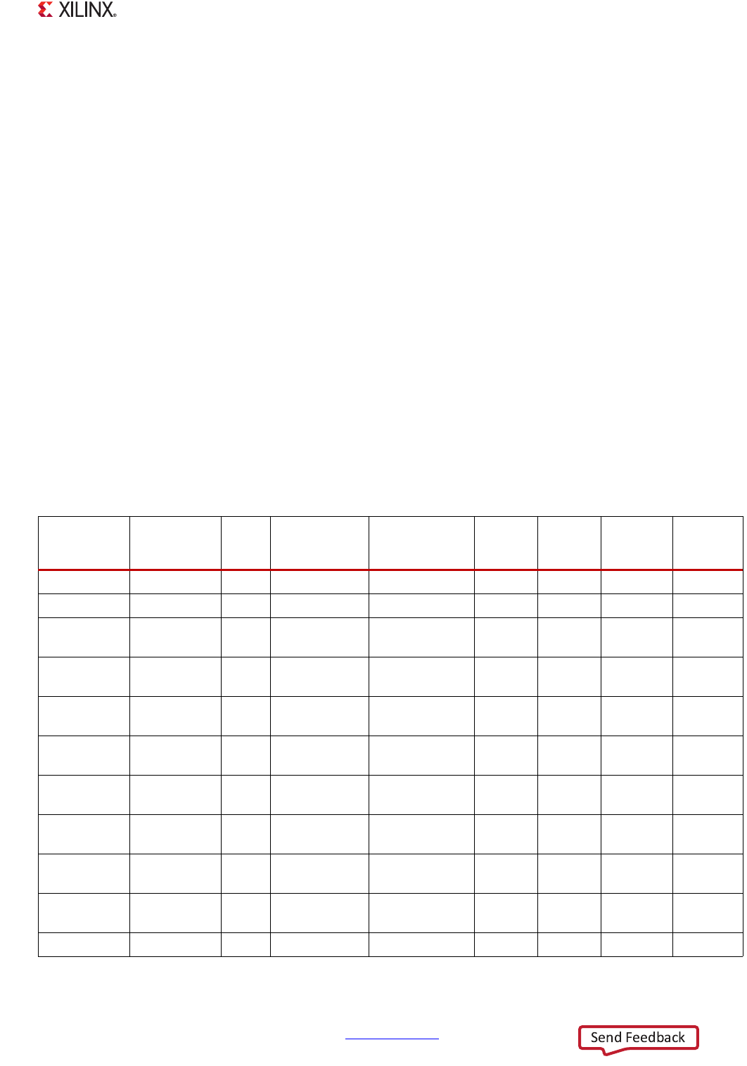
Table 5-1 lists the major datapaths used by the PS interconnect.
Table 5-1: Interconnect Datapaths
Source Destination Type
Clock
at source
Clock
at destination
Sync
or
Async
(1)
Data
width
R/W
Request
Capability
Advanced
QoS
CPU SCU AXI CPU_6x4x CPU_6x4x Sync 64 7, 12 -
AXI_ACP SCU AXI SAXIACPACLK CPU_6x4x Async 64 7, 3 -
AXI_HP FIFO AXI SAXIHPnACLK DDR_2x Async 32/64
14-70,
8-32
(2)
-
S_AXI_GP
Master
interconnect
AXI SAXIGPnACLK CPU_2x Async 32 8, 8 -
DevC
Master
interconnect
AXI CPU_1x CPU_2x Sync 32 8, 4 -
DAP
Master
interconnect
AHB CPU_1x CPU_2x Sync 32 1, 1 -
AHB masters
Central
interconnect
AXI CPU_1x CPU_2x Sync 32 8, 8 X
DMA
controller
Central
interconnect
AXI CPU_2x CPU_2x Sync 64 8, 8 X
Master
interconnect
Central
interconnect
AXI CPU_2x CPU_2x Sync 64 - -
FIFO
Memory
interconnect
AXI DDR_2x DDR_2x Sync 64 8, 8 -
SCU L2 Cache AXI CPU_6X4x CPU_6x4x Sync 64 8, 3 -