
User manual


Table Of Contents
- Zynq-7000 All Programmable SoC
- Table of Contents
- Ch. 1: Introduction
- Ch. 2: Signals, Interfaces, and Pins
- Ch. 3: Application Processing Unit
- Ch. 4: System Addresses
- Ch. 5: Interconnect
- Ch. 6: Boot and Configuration
- Ch. 7: Interrupts
- Ch. 8: Timers
- Ch. 9: DMA Controller
- Introduction
- Functional Description
- DMA Transfers on the AXI Interconnect
- AXI Transaction Considerations
- DMA Manager
- Multi-channel Data FIFO (MFIFO)
- Memory-to-Memory Transfers
- PL Peripheral AXI Transactions
- PL Peripheral Request Interface
- PL Peripheral - Length Managed by PL Peripheral
- PL Peripheral - Length Managed by DMAC
- Events and Interrupts
- Aborts
- Security
- IP Configuration Options
- Programming Guide for DMA Controller
- Programming Guide for DMA Engine
- Programming Restrictions
- System Functions
- I/O Interface
- Ch. 10: DDR Memory Controller
- Introduction
- AXI Memory Port Interface (DDRI)
- DDR Core and Transaction Scheduler (DDRC)
- DDRC Arbitration
- Controller PHY (DDRP)
- Initialization and Calibration
- DDR Clock Initialization
- DDR IOB Impedance Calibration
- DDR IOB Configuration
- DDR Controller Register Programming
- DRAM Reset and Initialization
- DRAM Input Impedance (ODT) Calibration
- DRAM Output Impedance (RON) Calibration
- DRAM Training
- Write Data Eye Adjustment
- Alternatives to Automatic DRAM Training
- DRAM Write Latency Restriction
- Register Overview
- Error Correction Code (ECC)
- Programming Model
- Ch. 11: Static Memory Controller
- Ch. 12: Quad-SPI Flash Controller
- Ch. 13: SD/SDIO Controller
- Ch. 14: General Purpose I/O (GPIO)
- Ch. 15: USB Host, Device, and OTG Controller
- Introduction
- Functional Description
- Programming Overview and Reference
- Device Mode Control
- Device Endpoint Data Structures
- Device Endpoint Packet Operational Model
- Device Endpoint Descriptor Reference
- Programming Guide for Device Controller
- Programming Guide for Device Endpoint Data Structures
- Host Mode Data Structures
- EHCI Implementation
- Host Data Structures Reference
- Programming Guide for Host Controller
- OTG Description and Reference
- System Functions
- I/O Interfaces
- Ch. 16: Gigabit Ethernet Controller
- Ch. 17: SPI Controller
- Ch. 18: CAN Controller
- Ch. 19: UART Controller
- Ch. 20: I2C Controller
- Ch. 21: Programmable Logic Description
- Ch. 22: Programmable Logic Design Guide
- Ch. 23: Programmable Logic Test and Debug
- Ch. 24: Power Management
- Ch. 25: Clocks
- Ch. 26: Reset System
- Ch. 27: JTAG and DAP Subsystem
- Ch. 28: System Test and Debug
- Ch. 29: On-Chip Memory (OCM)
- Ch. 30: XADC Interface
- Ch. 31: PCI Express
- Ch. 32: Device Secure Boot
- Appx. A: Additional Resources
- Appx. B: Register Details
- Overview
- Acronyms
- Module Summary
- AXI_HP Interface (AFI) (axi_hp)
- CAN Controller (can)
- DDR Memory Controller (ddrc)
- CoreSight Cross Trigger Interface (cti)
- Performance Monitor Unit (cortexa9_pmu)
- CoreSight Program Trace Macrocell (ptm)
- Debug Access Port (dap)
- CoreSight Embedded Trace Buffer (etb)
- PL Fabric Trace Monitor (ftm)
- CoreSight Trace Funnel (funnel)
- CoreSight Intstrumentation Trace Macrocell (itm)
- CoreSight Trace Packet Output (tpiu)
- Device Configuration Interface (devcfg)
- DMA Controller (dmac)
- Gigabit Ethernet Controller (GEM)
- General Purpose I/O (gpio)
- Interconnect QoS (qos301)
- NIC301 Address Region Control (nic301_addr_region_ctrl_registers)
- I2C Controller (IIC)
- L2 Cache (L2Cpl310)
- Application Processing Unit (mpcore)
- On-Chip Memory (ocm)
- Quad-SPI Flash Controller (qspi)
- SD Controller (sdio)
- System Level Control Registers (slcr)
- Static Memory Controller (pl353)
- SPI Controller (SPI)
- System Watchdog Timer (swdt)
- Triple Timer Counter (ttc)
- UART Controller (UART)
- USB Controller (usb)
Zynq-7000 AP SoC Technical Reference Manual www.xilinx.com 132
UG585 (v1.11) September 27, 2016
Chapter 5: Interconnect
QoS Priority
The AXI QoS input signals can be used to assign an arbitration priority to the read and write
commands.
Note that the PS interconnect allows either master control or programmable (register) control as a
configuration option. For the AFI, it is desirable to have the ability for masters to dynamically change
the QOS inputs. However, to provide flexibility the register field axi_hp.AFI_RDCHAN_CTRL
[FabricQosEn] is provided. This allows a static QoS value to be programmed through the high
performance AXI interface port, ignoring the PL AXI QoS inputs.
FIFO Occupancy
The level of the data and command FIFOs for both read and write are exported to the PL, allowing
you to take advantage of the QOS feature supported by the top-level interconnect. Based on the
relative levels of these FIFOs, a PL controller could dynamically change the priority of the individual
read and write requests into the high performance AXI interface block(s). For example, if a particular
PL master read data FIFO is getting too empty, the priority of the read requests could be increased.
The filling of this FIFO now takes priority over the other three FIFOs. When the FIFO reaches an
acceptable fill-level, the priority typically is reduced again. The exact scheme used to control the
relative priorities is flexible, as it must be performed in the programmable logic. Note that the “FIFO
Level” should be used as a relative level, as opposed to an exact level, because clock domain crossing
is involved.
Another possible application of the FIFO levels is using them to “look ahead” at the data fill level to
determine if data can be read or written without having to use AXI RVALID/WREADY handshake
signals. This could potentially simplify the AXI interface design logic, enabling higher speeds of
operation.
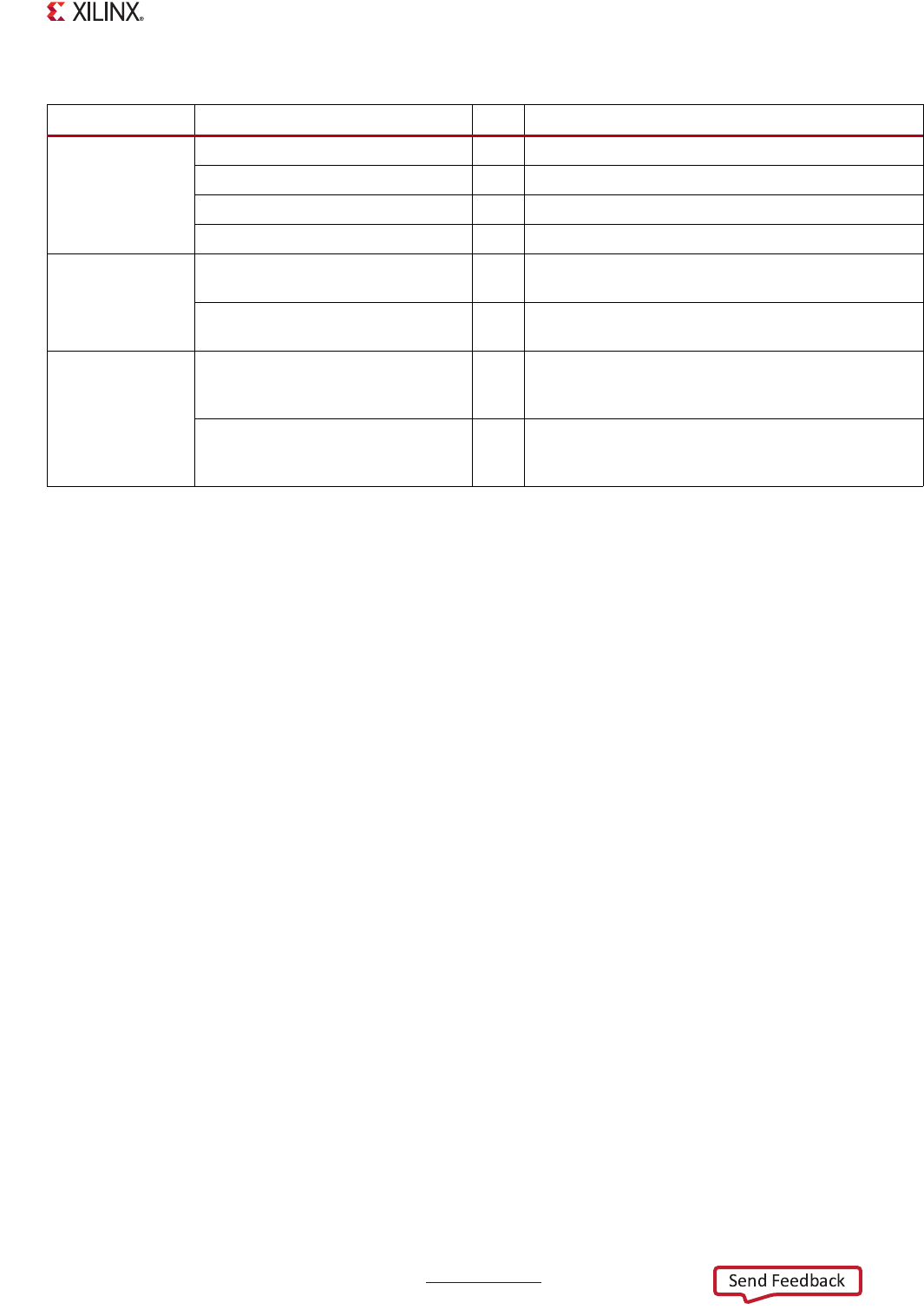
Table 5-7: Additional per-port HP PL Signals
Type PS-PL Signal Name I/O Description
FIFO occupancy
SAXIHP{0-3}RCOUNT[7:0] O Fill level of the RdData channel FIFO
SAXIHP{0-3}WCOUNT[7:0] O Fill level of the WrData channel FIFO
SAXIHP{0-3}RACOUNT[2:0] O Fill level of the RdAddr channel FIFO
SAXIHP{0-3}WACOUNT[5:0] O Fill level of the WrAddr channel FIFO
Quality of service
SAXIHP{0-3}AWQOS[3:0] I
WrAddr channel QOS input. Qualified by
SAXIHP{0-3}AWVALID
SAXIHP{0-3}ARQOS[3:0] I
RdAddr channel QOS input. Qualified by
SAXIHP{0-3}ARVALID
Interconnect
issuance
throttling
SAXIHP{0-3}RDISSUECAP1EN I
When asserted (1), indicates that the maximum
outstanding read commands (issuing capability)
should be derived from the “rdIssueCap1” register.
SAXIHP{0-3}WRISSUECAP1EN I
When asserted (1), indicates that the maximum
outstanding write commands (issuing capability)
should be derived from the “wrIssueCap1” register.