
User manual


Table Of Contents
- Zynq-7000 All Programmable SoC
- Table of Contents
- Ch. 1: Introduction
- Ch. 2: Signals, Interfaces, and Pins
- Ch. 3: Application Processing Unit
- Ch. 4: System Addresses
- Ch. 5: Interconnect
- Ch. 6: Boot and Configuration
- Ch. 7: Interrupts
- Ch. 8: Timers
- Ch. 9: DMA Controller
- Introduction
- Functional Description
- DMA Transfers on the AXI Interconnect
- AXI Transaction Considerations
- DMA Manager
- Multi-channel Data FIFO (MFIFO)
- Memory-to-Memory Transfers
- PL Peripheral AXI Transactions
- PL Peripheral Request Interface
- PL Peripheral - Length Managed by PL Peripheral
- PL Peripheral - Length Managed by DMAC
- Events and Interrupts
- Aborts
- Security
- IP Configuration Options
- Programming Guide for DMA Controller
- Programming Guide for DMA Engine
- Programming Restrictions
- System Functions
- I/O Interface
- Ch. 10: DDR Memory Controller
- Introduction
- AXI Memory Port Interface (DDRI)
- DDR Core and Transaction Scheduler (DDRC)
- DDRC Arbitration
- Controller PHY (DDRP)
- Initialization and Calibration
- DDR Clock Initialization
- DDR IOB Impedance Calibration
- DDR IOB Configuration
- DDR Controller Register Programming
- DRAM Reset and Initialization
- DRAM Input Impedance (ODT) Calibration
- DRAM Output Impedance (RON) Calibration
- DRAM Training
- Write Data Eye Adjustment
- Alternatives to Automatic DRAM Training
- DRAM Write Latency Restriction
- Register Overview
- Error Correction Code (ECC)
- Programming Model
- Ch. 11: Static Memory Controller
- Ch. 12: Quad-SPI Flash Controller
- Ch. 13: SD/SDIO Controller
- Ch. 14: General Purpose I/O (GPIO)
- Ch. 15: USB Host, Device, and OTG Controller
- Introduction
- Functional Description
- Programming Overview and Reference
- Device Mode Control
- Device Endpoint Data Structures
- Device Endpoint Packet Operational Model
- Device Endpoint Descriptor Reference
- Programming Guide for Device Controller
- Programming Guide for Device Endpoint Data Structures
- Host Mode Data Structures
- EHCI Implementation
- Host Data Structures Reference
- Programming Guide for Host Controller
- OTG Description and Reference
- System Functions
- I/O Interfaces
- Ch. 16: Gigabit Ethernet Controller
- Ch. 17: SPI Controller
- Ch. 18: CAN Controller
- Ch. 19: UART Controller
- Ch. 20: I2C Controller
- Ch. 21: Programmable Logic Description
- Ch. 22: Programmable Logic Design Guide
- Ch. 23: Programmable Logic Test and Debug
- Ch. 24: Power Management
- Ch. 25: Clocks
- Ch. 26: Reset System
- Ch. 27: JTAG and DAP Subsystem
- Ch. 28: System Test and Debug
- Ch. 29: On-Chip Memory (OCM)
- Ch. 30: XADC Interface
- Ch. 31: PCI Express
- Ch. 32: Device Secure Boot
- Appx. A: Additional Resources
- Appx. B: Register Details
- Overview
- Acronyms
- Module Summary
- AXI_HP Interface (AFI) (axi_hp)
- CAN Controller (can)
- DDR Memory Controller (ddrc)
- CoreSight Cross Trigger Interface (cti)
- Performance Monitor Unit (cortexa9_pmu)
- CoreSight Program Trace Macrocell (ptm)
- Debug Access Port (dap)
- CoreSight Embedded Trace Buffer (etb)
- PL Fabric Trace Monitor (ftm)
- CoreSight Trace Funnel (funnel)
- CoreSight Intstrumentation Trace Macrocell (itm)
- CoreSight Trace Packet Output (tpiu)
- Device Configuration Interface (devcfg)
- DMA Controller (dmac)
- Gigabit Ethernet Controller (GEM)
- General Purpose I/O (gpio)
- Interconnect QoS (qos301)
- NIC301 Address Region Control (nic301_addr_region_ctrl_registers)
- I2C Controller (IIC)
- L2 Cache (L2Cpl310)
- Application Processing Unit (mpcore)
- On-Chip Memory (ocm)
- Quad-SPI Flash Controller (qspi)
- SD Controller (sdio)
- System Level Control Registers (slcr)
- Static Memory Controller (pl353)
- SPI Controller (SPI)
- System Watchdog Timer (swdt)
- Triple Timer Counter (ttc)
- UART Controller (UART)
- USB Controller (usb)
Zynq-7000 AP SoC Technical Reference Manual www.xilinx.com 150
UG585 (v1.11) September 27, 2016
Chapter 6: Boot and Configuration
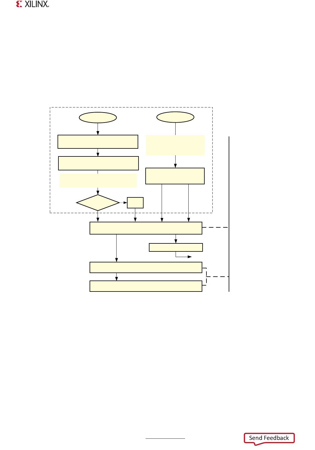
Device Boot Flowchart
The POR reset causes the hardware to samples the pin straps, disable modules in the device, and
optionally enables the PS clock PLLs. These hardware actions are not performed after a non-POR
reset.
The first software to run is the BootROM, then the FSBL/User code and system code. All of these
steps are shown in Figure 6-1.
BootROM and Header Parameters
The BootROM header includes a dozen parameters that guide the BootROM execution flow. For
example, the header includes a parameter to select the security mode: the Encryption Status
parameter. In secure mode, the FSBL/User code, bitstream, and other software are encrypted. The
BootROM has the ability to authenticate and decrypt the encrypted FSBL/User code. The header
itself is never encrypted.
As another example, the header includes the Length of Image parameter that defines the length of
the FSBL/User code that the BootROM loads into the OCM for execution. This code is limited to
192 KB in length. This parameter can be set to zero to indicate the desire to execute code directly
X-Ref Target - Figure 6-1
Figure 6-1: PS/PL Boot Process for Hardware and Software
325
1RQ325
5HVHWDOO5HJLVWHUV
+DUGZDUH6DPSOHV0RGHB3LQV
-7$*,23''5HWF
FRQWUROOHUVDUHGLVDEOHG
5HVHWVDOOUHJLVWHUVH[FHSW
WKHSHUVLVWHQWUHJLVWHUV
:LWKRUZLWKRXW
3RZHUXS
1RQ
6HFXUH
3//%\SDVV"
%RRW520([HFXWHV
(QDEOH
3//V
2SHUDWLQJ6\VWHP
)6%/8VHU&RGH
/RFNGRZQ
6HFXUH
,QLWLDOL]H&RQILJXUH(QDEOH
7KH)6%/8VHU$SSOLFDWLRQ
FRGHFDQFOHDUSURJUDPDQG
HQDEOHWKH3/
36+DUGZDUH)XQFWLRQV
)DLOXUH6XFFHVV
7KLVFRXOGEHDVHFXUH%RRW0RGH7KHPRGH
ZLOOEHGHWHUPLQHGE\WKH%RRW520XVLQJWKH
KHDGHU(QFU\SWLRQ6WDWXVSDUDPHWHU
6WDUWXS3RZHUXS
7KH3/KDUGZDUHLQFOXGHVD
VHOIVWDUWXSVHTXHQFHWR
SUHSDUHLWIRULQLWLDOL]DWLRQE\
WKH%RRW520RU8VHUFRGH
(UURU&RGH*HQHUDWHG
,QLWLDOL]H
7KH3/PXVWEHSRZHUHGXS
IRU6HFXUHPRGHRULIWKH
-7$*LQWHUIDFHLVUHTXLUHG
6WDJH
6WDJH
6WDJH
8*BFBB
3/7LPHOLQH
1R
<HV
5HWDLQWKHSUHYLRXV%RRW0RGHDV
6HFXUHRU1RQ6HFXUHXVLQJWKH
GHYFIJ&75/>6(&B(1@UHJLVWHUELW
IRUDFFHVVE\WKH%RRW520