
User manual


Table Of Contents
- Zynq-7000 All Programmable SoC
- Table of Contents
- Ch. 1: Introduction
- Ch. 2: Signals, Interfaces, and Pins
- Ch. 3: Application Processing Unit
- Ch. 4: System Addresses
- Ch. 5: Interconnect
- Ch. 6: Boot and Configuration
- Ch. 7: Interrupts
- Ch. 8: Timers
- Ch. 9: DMA Controller
- Introduction
- Functional Description
- DMA Transfers on the AXI Interconnect
- AXI Transaction Considerations
- DMA Manager
- Multi-channel Data FIFO (MFIFO)
- Memory-to-Memory Transfers
- PL Peripheral AXI Transactions
- PL Peripheral Request Interface
- PL Peripheral - Length Managed by PL Peripheral
- PL Peripheral - Length Managed by DMAC
- Events and Interrupts
- Aborts
- Security
- IP Configuration Options
- Programming Guide for DMA Controller
- Programming Guide for DMA Engine
- Programming Restrictions
- System Functions
- I/O Interface
- Ch. 10: DDR Memory Controller
- Introduction
- AXI Memory Port Interface (DDRI)
- DDR Core and Transaction Scheduler (DDRC)
- DDRC Arbitration
- Controller PHY (DDRP)
- Initialization and Calibration
- DDR Clock Initialization
- DDR IOB Impedance Calibration
- DDR IOB Configuration
- DDR Controller Register Programming
- DRAM Reset and Initialization
- DRAM Input Impedance (ODT) Calibration
- DRAM Output Impedance (RON) Calibration
- DRAM Training
- Write Data Eye Adjustment
- Alternatives to Automatic DRAM Training
- DRAM Write Latency Restriction
- Register Overview
- Error Correction Code (ECC)
- Programming Model
- Ch. 11: Static Memory Controller
- Ch. 12: Quad-SPI Flash Controller
- Ch. 13: SD/SDIO Controller
- Ch. 14: General Purpose I/O (GPIO)
- Ch. 15: USB Host, Device, and OTG Controller
- Introduction
- Functional Description
- Programming Overview and Reference
- Device Mode Control
- Device Endpoint Data Structures
- Device Endpoint Packet Operational Model
- Device Endpoint Descriptor Reference
- Programming Guide for Device Controller
- Programming Guide for Device Endpoint Data Structures
- Host Mode Data Structures
- EHCI Implementation
- Host Data Structures Reference
- Programming Guide for Host Controller
- OTG Description and Reference
- System Functions
- I/O Interfaces
- Ch. 16: Gigabit Ethernet Controller
- Ch. 17: SPI Controller
- Ch. 18: CAN Controller
- Ch. 19: UART Controller
- Ch. 20: I2C Controller
- Ch. 21: Programmable Logic Description
- Ch. 22: Programmable Logic Design Guide
- Ch. 23: Programmable Logic Test and Debug
- Ch. 24: Power Management
- Ch. 25: Clocks
- Ch. 26: Reset System
- Ch. 27: JTAG and DAP Subsystem
- Ch. 28: System Test and Debug
- Ch. 29: On-Chip Memory (OCM)
- Ch. 30: XADC Interface
- Ch. 31: PCI Express
- Ch. 32: Device Secure Boot
- Appx. A: Additional Resources
- Appx. B: Register Details
- Overview
- Acronyms
- Module Summary
- AXI_HP Interface (AFI) (axi_hp)
- CAN Controller (can)
- DDR Memory Controller (ddrc)
- CoreSight Cross Trigger Interface (cti)
- Performance Monitor Unit (cortexa9_pmu)
- CoreSight Program Trace Macrocell (ptm)
- Debug Access Port (dap)
- CoreSight Embedded Trace Buffer (etb)
- PL Fabric Trace Monitor (ftm)
- CoreSight Trace Funnel (funnel)
- CoreSight Intstrumentation Trace Macrocell (itm)
- CoreSight Trace Packet Output (tpiu)
- Device Configuration Interface (devcfg)
- DMA Controller (dmac)
- Gigabit Ethernet Controller (GEM)
- General Purpose I/O (gpio)
- Interconnect QoS (qos301)
- NIC301 Address Region Control (nic301_addr_region_ctrl_registers)
- I2C Controller (IIC)
- L2 Cache (L2Cpl310)
- Application Processing Unit (mpcore)
- On-Chip Memory (ocm)
- Quad-SPI Flash Controller (qspi)
- SD Controller (sdio)
- System Level Control Registers (slcr)
- Static Memory Controller (pl353)
- SPI Controller (SPI)
- System Watchdog Timer (swdt)
- Triple Timer Counter (ttc)
- UART Controller (UART)
- USB Controller (usb)
Zynq-7000 AP SoC Technical Reference Manual www.xilinx.com 163
UG585 (v1.11) September 27, 2016
Chapter 6: Boot and Configuration
External Reset Signal Pins
There are two external reset pins:
• PS_POR_B: This reset is used to hold the PS in reset until all PS power supplies are at the
required voltage levels. It must be held Low during PS power supply ramp-up. PS_POR_B can be
generated by the power supply “power-good” signal. The POR reset is the only reset to sample
the boot mode pin strap resistors.
Note: PS_POR_B must not be de-asserted during a certain timing window relative to when the
last PL power supply starts to ramp. Asserting PS_POR_B during this window can cause a
lock-down event. Refer to section 6.3.3 BootROM Performance: PS_POR_B De-assertion
Guidelines, page 177 for more details.
• PS_SRST_B: This reset is used to force a system reset. It can be tied or pulled High, and can be
High during the PS power supply ramp-up. The PS_SRST_B reset is a non-POR reset.
Note: The PS_SRST_B signal must not be asserted while the BootROM is executing from a POR
reset, otherwise a lock-down event occurs and prevents the BootROM from completing the
system boot process. To recover from this type of lockdown, the PS_POR_B reset must be
asserted. The time taken by Boot ROM to complete its execution and handoff to the FSBL/user
application depends on the several factors. Please refer to Boot Time Reference, page 220 for
details on how to arrive at the boot time for a specific user configuration.
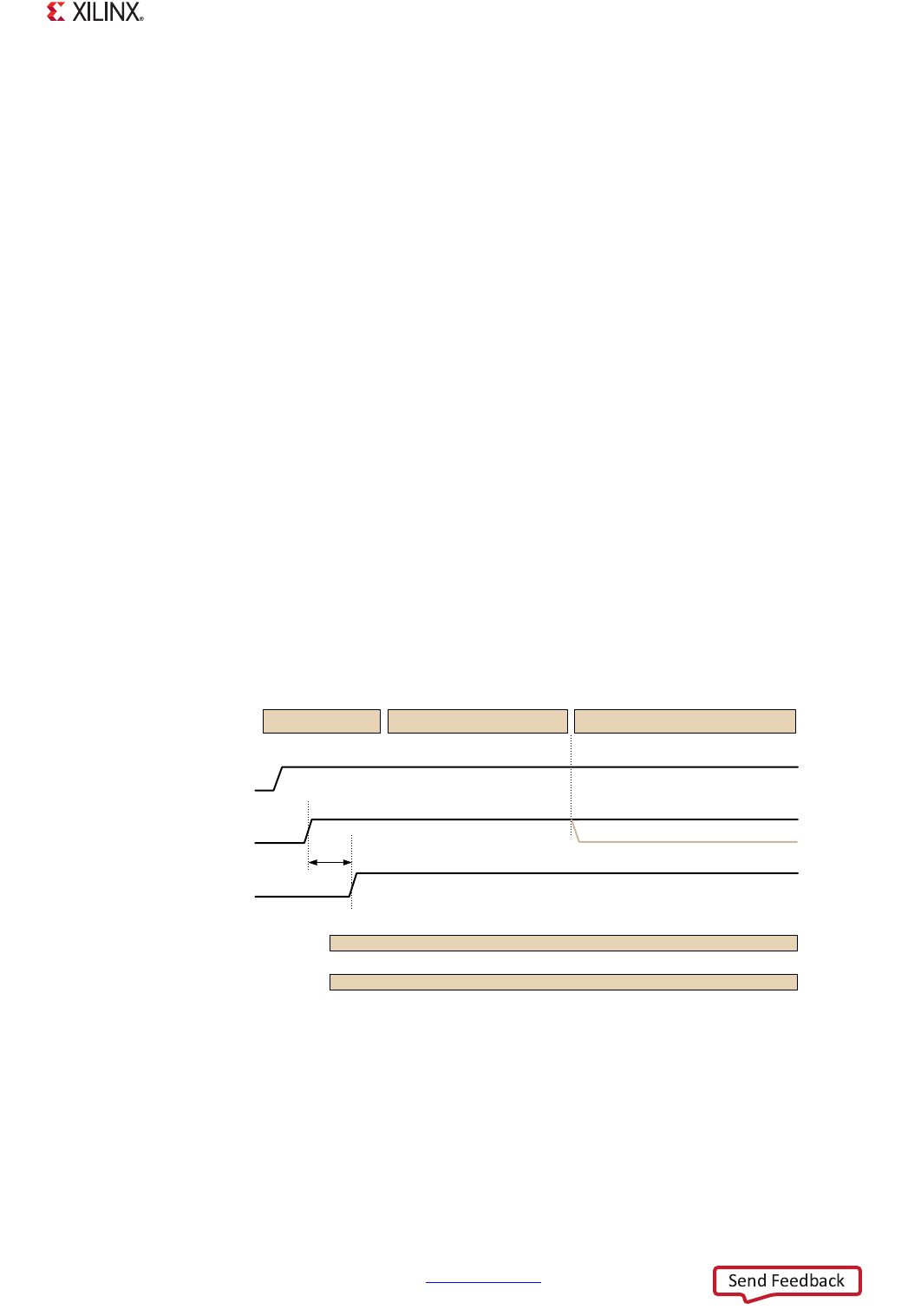
Reset Signal Sequencing
The reset sequencing required for boot are illustrated in Figure 6-4. The effects of the resets are
described in this chapter and in Chapter 26, Reset System. If PS_SRST_B is asserted while the
BootROM is executing, then a system lockdown occurs without an error code being generated.
X-Ref Target - Figure 6-4
Figure 6-4: Power and Reset Sequencing Waveform
363/SRZHU
36B&/.
3//HQDEOHG
36B6567B%
36B325B%
36B&/.
3//E\SDVV
6WDEOH+LJK)UHT&ORFN
WR0+]&ORFN7UDQVLWLRQV
%RRW520([HFXWHV
0LQLPXPRIwV
36B6567B%PXVWVWD\+LJK
+DUGZDUH )6%/8VHU&RGH26
8*BFBB
36B6567B%FDQEHGULYHQ/RZWRUHVHW
WKHV\VWHPDIWHU%RRW520H[HFXWHV