
User manual


Table Of Contents
- Zynq-7000 All Programmable SoC
- Table of Contents
- Ch. 1: Introduction
- Ch. 2: Signals, Interfaces, and Pins
- Ch. 3: Application Processing Unit
- Ch. 4: System Addresses
- Ch. 5: Interconnect
- Ch. 6: Boot and Configuration
- Ch. 7: Interrupts
- Ch. 8: Timers
- Ch. 9: DMA Controller
- Introduction
- Functional Description
- DMA Transfers on the AXI Interconnect
- AXI Transaction Considerations
- DMA Manager
- Multi-channel Data FIFO (MFIFO)
- Memory-to-Memory Transfers
- PL Peripheral AXI Transactions
- PL Peripheral Request Interface
- PL Peripheral - Length Managed by PL Peripheral
- PL Peripheral - Length Managed by DMAC
- Events and Interrupts
- Aborts
- Security
- IP Configuration Options
- Programming Guide for DMA Controller
- Programming Guide for DMA Engine
- Programming Restrictions
- System Functions
- I/O Interface
- Ch. 10: DDR Memory Controller
- Introduction
- AXI Memory Port Interface (DDRI)
- DDR Core and Transaction Scheduler (DDRC)
- DDRC Arbitration
- Controller PHY (DDRP)
- Initialization and Calibration
- DDR Clock Initialization
- DDR IOB Impedance Calibration
- DDR IOB Configuration
- DDR Controller Register Programming
- DRAM Reset and Initialization
- DRAM Input Impedance (ODT) Calibration
- DRAM Output Impedance (RON) Calibration
- DRAM Training
- Write Data Eye Adjustment
- Alternatives to Automatic DRAM Training
- DRAM Write Latency Restriction
- Register Overview
- Error Correction Code (ECC)
- Programming Model
- Ch. 11: Static Memory Controller
- Ch. 12: Quad-SPI Flash Controller
- Ch. 13: SD/SDIO Controller
- Ch. 14: General Purpose I/O (GPIO)
- Ch. 15: USB Host, Device, and OTG Controller
- Introduction
- Functional Description
- Programming Overview and Reference
- Device Mode Control
- Device Endpoint Data Structures
- Device Endpoint Packet Operational Model
- Device Endpoint Descriptor Reference
- Programming Guide for Device Controller
- Programming Guide for Device Endpoint Data Structures
- Host Mode Data Structures
- EHCI Implementation
- Host Data Structures Reference
- Programming Guide for Host Controller
- OTG Description and Reference
- System Functions
- I/O Interfaces
- Ch. 16: Gigabit Ethernet Controller
- Ch. 17: SPI Controller
- Ch. 18: CAN Controller
- Ch. 19: UART Controller
- Ch. 20: I2C Controller
- Ch. 21: Programmable Logic Description
- Ch. 22: Programmable Logic Design Guide
- Ch. 23: Programmable Logic Test and Debug
- Ch. 24: Power Management
- Ch. 25: Clocks
- Ch. 26: Reset System
- Ch. 27: JTAG and DAP Subsystem
- Ch. 28: System Test and Debug
- Ch. 29: On-Chip Memory (OCM)
- Ch. 30: XADC Interface
- Ch. 31: PCI Express
- Ch. 32: Device Secure Boot
- Appx. A: Additional Resources
- Appx. B: Register Details
- Overview
- Acronyms
- Module Summary
- AXI_HP Interface (AFI) (axi_hp)
- CAN Controller (can)
- DDR Memory Controller (ddrc)
- CoreSight Cross Trigger Interface (cti)
- Performance Monitor Unit (cortexa9_pmu)
- CoreSight Program Trace Macrocell (ptm)
- Debug Access Port (dap)
- CoreSight Embedded Trace Buffer (etb)
- PL Fabric Trace Monitor (ftm)
- CoreSight Trace Funnel (funnel)
- CoreSight Intstrumentation Trace Macrocell (itm)
- CoreSight Trace Packet Output (tpiu)
- Device Configuration Interface (devcfg)
- DMA Controller (dmac)
- Gigabit Ethernet Controller (GEM)
- General Purpose I/O (gpio)
- Interconnect QoS (qos301)
- NIC301 Address Region Control (nic301_addr_region_ctrl_registers)
- I2C Controller (IIC)
- L2 Cache (L2Cpl310)
- Application Processing Unit (mpcore)
- On-Chip Memory (ocm)
- Quad-SPI Flash Controller (qspi)
- SD Controller (sdio)
- System Level Control Registers (slcr)
- Static Memory Controller (pl353)
- SPI Controller (SPI)
- System Watchdog Timer (swdt)
- Triple Timer Counter (ttc)
- UART Controller (UART)
- USB Controller (usb)
Zynq-7000 AP SoC Technical Reference Manual www.xilinx.com 164
UG585 (v1.11) September 27, 2016
Chapter 6: Boot and Configuration
Internal Resets
The internal resets are all non-POR resets. Resets are described in Chapter 26, Reset System.
• Software controlled reset: write 1 to slcr.PSS_RST_CTRL [SOFT_RST].
• Watchdog timers: AWDT0, AWDT1, and SWDT controllers.
• JTAG interface and debug.
Reset Reason
The type of reset that last occurred (reset reason) is recorded in the slcr.REBOOT_STATUS register.
This register also includes the BootROM error code, when it is generated. The register is accessible
to the BootROM and FSBL/User code. The Reboot Status register is reset by a POR reset, but
preserved by a non-POR reset.
System Reset Effects
The effects of the system resets (POR and non-POR) are summarized in Table 6-3.
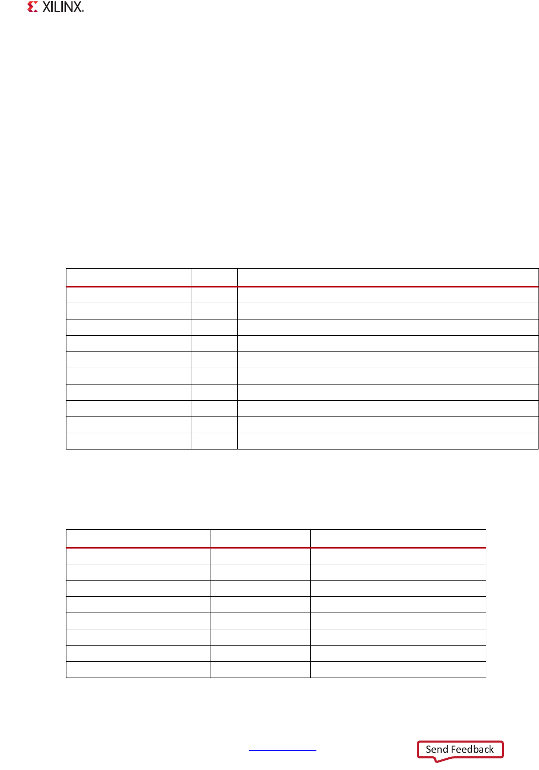
Table 6-2: Reboot Status Register
slcr.REBOOT_STATUS
Bit Source
[REBOOT_STATE] 31:24 R/W bit field that remains persistent through all non-POR resets.
Reserved 23 Reserved.
[POR] 22 PS_POR_B reset signal. This is the only reset set after a POR reset.
[SRST_B] 21 PS_SRST_B reset signal.
[DBG_RST] 20 Debug command in the DAP controller.
[SLC_RST] 19 Write to the slcr.PSS_RST_CTRL [SOFT_RST] bit.
[AWDT1_RST] 18 CPU 1 watchdog timer.
[AWDT0_RST] 17 CPU 0 watchdog timer.
[SWDT_RST] 16 System watchdog timer.
[BOOTROM_ERROR_CODE] 15:0 BootROM, refer to Table 6-20.
Table 6-3: System Reset Effects
Reset Type POR Non-POR
Sample Pin Straps Yes No
Initialize PS PLLs
(1)
Yes, by the hardware Yes, by the BootROM
PS RAM (FIFOs, buffers, etc.) Cleared Cleared
IOP clocks Disabled Disabled
BootROM executes Yes Yes
Retains previous boot mode No Yes
Reboot Status register Resets it Accumulates the system reset type.
Device Registers All Persistent registers.
(2)