
User manual


Table Of Contents
- Zynq-7000 All Programmable SoC
- Table of Contents
- Ch. 1: Introduction
- Ch. 2: Signals, Interfaces, and Pins
- Ch. 3: Application Processing Unit
- Ch. 4: System Addresses
- Ch. 5: Interconnect
- Ch. 6: Boot and Configuration
- Ch. 7: Interrupts
- Ch. 8: Timers
- Ch. 9: DMA Controller
- Introduction
- Functional Description
- DMA Transfers on the AXI Interconnect
- AXI Transaction Considerations
- DMA Manager
- Multi-channel Data FIFO (MFIFO)
- Memory-to-Memory Transfers
- PL Peripheral AXI Transactions
- PL Peripheral Request Interface
- PL Peripheral - Length Managed by PL Peripheral
- PL Peripheral - Length Managed by DMAC
- Events and Interrupts
- Aborts
- Security
- IP Configuration Options
- Programming Guide for DMA Controller
- Programming Guide for DMA Engine
- Programming Restrictions
- System Functions
- I/O Interface
- Ch. 10: DDR Memory Controller
- Introduction
- AXI Memory Port Interface (DDRI)
- DDR Core and Transaction Scheduler (DDRC)
- DDRC Arbitration
- Controller PHY (DDRP)
- Initialization and Calibration
- DDR Clock Initialization
- DDR IOB Impedance Calibration
- DDR IOB Configuration
- DDR Controller Register Programming
- DRAM Reset and Initialization
- DRAM Input Impedance (ODT) Calibration
- DRAM Output Impedance (RON) Calibration
- DRAM Training
- Write Data Eye Adjustment
- Alternatives to Automatic DRAM Training
- DRAM Write Latency Restriction
- Register Overview
- Error Correction Code (ECC)
- Programming Model
- Ch. 11: Static Memory Controller
- Ch. 12: Quad-SPI Flash Controller
- Ch. 13: SD/SDIO Controller
- Ch. 14: General Purpose I/O (GPIO)
- Ch. 15: USB Host, Device, and OTG Controller
- Introduction
- Functional Description
- Programming Overview and Reference
- Device Mode Control
- Device Endpoint Data Structures
- Device Endpoint Packet Operational Model
- Device Endpoint Descriptor Reference
- Programming Guide for Device Controller
- Programming Guide for Device Endpoint Data Structures
- Host Mode Data Structures
- EHCI Implementation
- Host Data Structures Reference
- Programming Guide for Host Controller
- OTG Description and Reference
- System Functions
- I/O Interfaces
- Ch. 16: Gigabit Ethernet Controller
- Ch. 17: SPI Controller
- Ch. 18: CAN Controller
- Ch. 19: UART Controller
- Ch. 20: I2C Controller
- Ch. 21: Programmable Logic Description
- Ch. 22: Programmable Logic Design Guide
- Ch. 23: Programmable Logic Test and Debug
- Ch. 24: Power Management
- Ch. 25: Clocks
- Ch. 26: Reset System
- Ch. 27: JTAG and DAP Subsystem
- Ch. 28: System Test and Debug
- Ch. 29: On-Chip Memory (OCM)
- Ch. 30: XADC Interface
- Ch. 31: PCI Express
- Ch. 32: Device Secure Boot
- Appx. A: Additional Resources
- Appx. B: Register Details
- Overview
- Acronyms
- Module Summary
- AXI_HP Interface (AFI) (axi_hp)
- CAN Controller (can)
- DDR Memory Controller (ddrc)
- CoreSight Cross Trigger Interface (cti)
- Performance Monitor Unit (cortexa9_pmu)
- CoreSight Program Trace Macrocell (ptm)
- Debug Access Port (dap)
- CoreSight Embedded Trace Buffer (etb)
- PL Fabric Trace Monitor (ftm)
- CoreSight Trace Funnel (funnel)
- CoreSight Intstrumentation Trace Macrocell (itm)
- CoreSight Trace Packet Output (tpiu)
- Device Configuration Interface (devcfg)
- DMA Controller (dmac)
- Gigabit Ethernet Controller (GEM)
- General Purpose I/O (gpio)
- Interconnect QoS (qos301)
- NIC301 Address Region Control (nic301_addr_region_ctrl_registers)
- I2C Controller (IIC)
- L2 Cache (L2Cpl310)
- Application Processing Unit (mpcore)
- On-Chip Memory (ocm)
- Quad-SPI Flash Controller (qspi)
- SD Controller (sdio)
- System Level Control Registers (slcr)
- Static Memory Controller (pl353)
- SPI Controller (SPI)
- System Watchdog Timer (swdt)
- Triple Timer Counter (ttc)
- UART Controller (UART)
- USB Controller (usb)
Zynq-7000 AP SoC Technical Reference Manual www.xilinx.com 166
UG585 (v1.11) September 27, 2016
Chapter 6: Boot and Configuration
6.2.6 I/O Pin Connections for Boot Devices
The BootROM expects certain external pins to be connected. Some pins connections are necessary
for all boot modes. Others depend on the boot mode pin straps and the BootROM Header. After the
BootROM executes, user code can reconfigure the I/O pin connections as desired.
• Connections required for all boot configurations:
°
PS power supply
°
PS_POR_B, PS_SRST_B, and PS_CLK_B
• MIO connections for specific boot devices
°
Quad-SPI (auto detect 1, 2, 4, or 8-bit interface)
°
SD memory card (SDIO 0, MIO pins 40-47)
°
NAND (auto detect 8 or 16-bit interface)
°
NOR (CS 0)
°
JTAG (PLJTAG interface), normally used in Cascade Chain mode
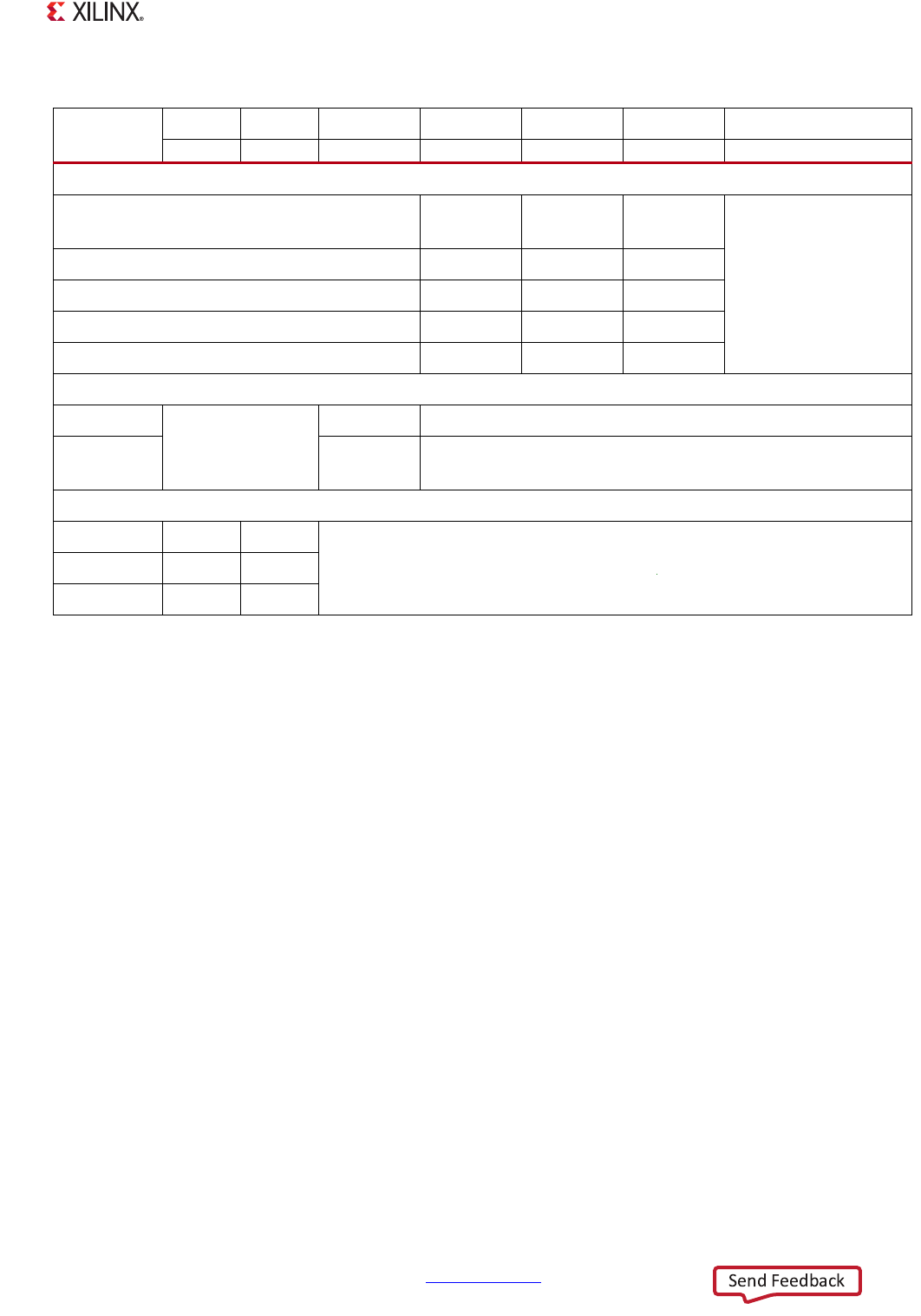
Table 6-4: Boot Mode MIO Strapping Pins
Pin-signal /
Mode
MIO[8] MIO[7] MIO[6] MIO[5] MIO[4] MIO[3] MIO[2]
VMODE[1] VMODE[0] BOOT_MODE[4] BOOT_MODE[0] BOOT_MODE[2] BOOT_MODE[1] BOOT_MODE[3]
Boot Devices
JTAG Boot Mode; cascaded is most
common
(1)
000
JTAG Chain Routing
(2)
0: Cascade mode
1: Independent mode
NOR Boot
(3)
001
NAND
010
Quad-SPI
(3)
100
SD Card
110
Mode for all 3 PLLs
PLL Enabled
0
Hardware waits for PLL to lock, then executes BootROM.
PLL
Bypassed
1
Allows for a wide PS_CLK frequency range.
MIO Bank Voltage
(4)
Bank 1 Bank 0
Voltage Bank 0 includes MIO pins 0 thru 15.
Voltage Bank 1 includes MIO pins 16 thru 53.
2.5 V, 3.3 V
00
1.8 V
11
Notes:
1. JTAG cascaded mode is most common and is the assumed mode in all the references to JTAG mode except where noted.
2. For secure mode, JTAG is not enabled and MIO[2] is ignored.
3. The Quad-SPI and NOR boot modes support execute-in-place (this support is always non-secure)
4. Voltage Banks 0 and 1 must be set to the same value when an interface spans across these voltage banks. Examples
include NOR, 16-bit NAND, and a wide TPIU test port. Other interface configuration may also span the two banks.