
User manual


Table Of Contents
- Zynq-7000 All Programmable SoC
- Table of Contents
- Ch. 1: Introduction
- Ch. 2: Signals, Interfaces, and Pins
- Ch. 3: Application Processing Unit
- Ch. 4: System Addresses
- Ch. 5: Interconnect
- Ch. 6: Boot and Configuration
- Ch. 7: Interrupts
- Ch. 8: Timers
- Ch. 9: DMA Controller
- Introduction
- Functional Description
- DMA Transfers on the AXI Interconnect
- AXI Transaction Considerations
- DMA Manager
- Multi-channel Data FIFO (MFIFO)
- Memory-to-Memory Transfers
- PL Peripheral AXI Transactions
- PL Peripheral Request Interface
- PL Peripheral - Length Managed by PL Peripheral
- PL Peripheral - Length Managed by DMAC
- Events and Interrupts
- Aborts
- Security
- IP Configuration Options
- Programming Guide for DMA Controller
- Programming Guide for DMA Engine
- Programming Restrictions
- System Functions
- I/O Interface
- Ch. 10: DDR Memory Controller
- Introduction
- AXI Memory Port Interface (DDRI)
- DDR Core and Transaction Scheduler (DDRC)
- DDRC Arbitration
- Controller PHY (DDRP)
- Initialization and Calibration
- DDR Clock Initialization
- DDR IOB Impedance Calibration
- DDR IOB Configuration
- DDR Controller Register Programming
- DRAM Reset and Initialization
- DRAM Input Impedance (ODT) Calibration
- DRAM Output Impedance (RON) Calibration
- DRAM Training
- Write Data Eye Adjustment
- Alternatives to Automatic DRAM Training
- DRAM Write Latency Restriction
- Register Overview
- Error Correction Code (ECC)
- Programming Model
- Ch. 11: Static Memory Controller
- Ch. 12: Quad-SPI Flash Controller
- Ch. 13: SD/SDIO Controller
- Ch. 14: General Purpose I/O (GPIO)
- Ch. 15: USB Host, Device, and OTG Controller
- Introduction
- Functional Description
- Programming Overview and Reference
- Device Mode Control
- Device Endpoint Data Structures
- Device Endpoint Packet Operational Model
- Device Endpoint Descriptor Reference
- Programming Guide for Device Controller
- Programming Guide for Device Endpoint Data Structures
- Host Mode Data Structures
- EHCI Implementation
- Host Data Structures Reference
- Programming Guide for Host Controller
- OTG Description and Reference
- System Functions
- I/O Interfaces
- Ch. 16: Gigabit Ethernet Controller
- Ch. 17: SPI Controller
- Ch. 18: CAN Controller
- Ch. 19: UART Controller
- Ch. 20: I2C Controller
- Ch. 21: Programmable Logic Description
- Ch. 22: Programmable Logic Design Guide
- Ch. 23: Programmable Logic Test and Debug
- Ch. 24: Power Management
- Ch. 25: Clocks
- Ch. 26: Reset System
- Ch. 27: JTAG and DAP Subsystem
- Ch. 28: System Test and Debug
- Ch. 29: On-Chip Memory (OCM)
- Ch. 30: XADC Interface
- Ch. 31: PCI Express
- Ch. 32: Device Secure Boot
- Appx. A: Additional Resources
- Appx. B: Register Details
- Overview
- Acronyms
- Module Summary
- AXI_HP Interface (AFI) (axi_hp)
- CAN Controller (can)
- DDR Memory Controller (ddrc)
- CoreSight Cross Trigger Interface (cti)
- Performance Monitor Unit (cortexa9_pmu)
- CoreSight Program Trace Macrocell (ptm)
- Debug Access Port (dap)
- CoreSight Embedded Trace Buffer (etb)
- PL Fabric Trace Monitor (ftm)
- CoreSight Trace Funnel (funnel)
- CoreSight Intstrumentation Trace Macrocell (itm)
- CoreSight Trace Packet Output (tpiu)
- Device Configuration Interface (devcfg)
- DMA Controller (dmac)
- Gigabit Ethernet Controller (GEM)
- General Purpose I/O (gpio)
- Interconnect QoS (qos301)
- NIC301 Address Region Control (nic301_addr_region_ctrl_registers)
- I2C Controller (IIC)
- L2 Cache (L2Cpl310)
- Application Processing Unit (mpcore)
- On-Chip Memory (ocm)
- Quad-SPI Flash Controller (qspi)
- SD Controller (sdio)
- System Level Control Registers (slcr)
- Static Memory Controller (pl353)
- SPI Controller (SPI)
- System Watchdog Timer (swdt)
- Triple Timer Counter (ttc)
- UART Controller (UART)
- USB Controller (usb)
Zynq-7000 AP SoC Technical Reference Manual www.xilinx.com 169
UG585 (v1.11) September 27, 2016
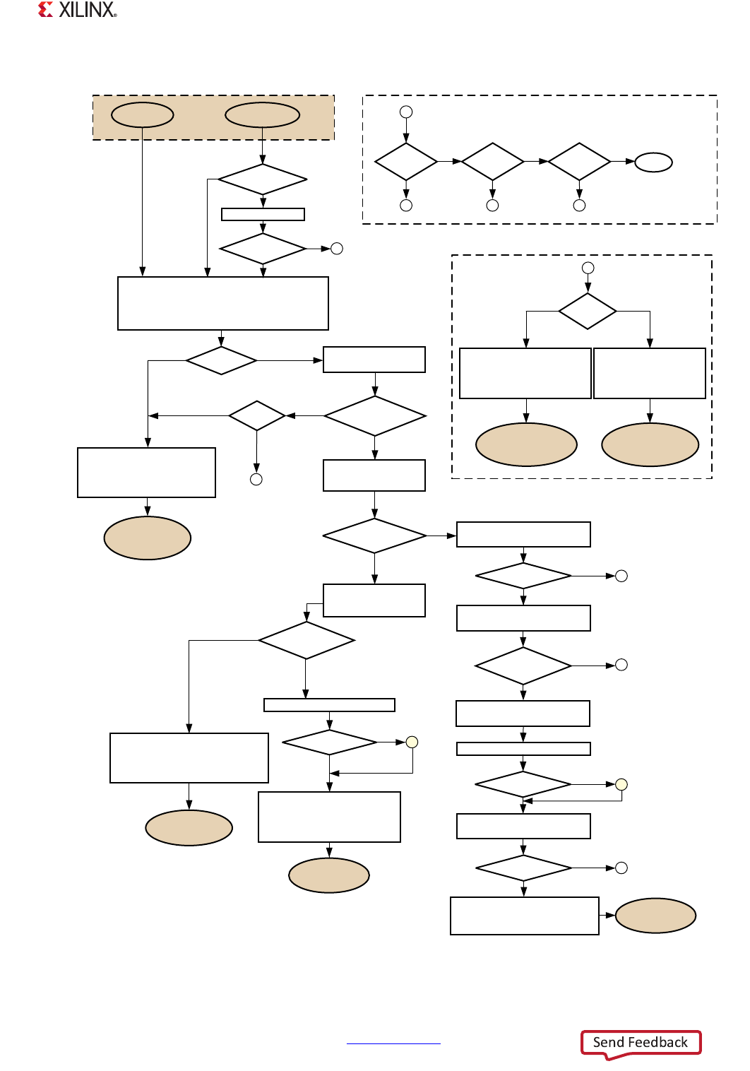
Chapter 6: Boot and Configuration
X-Ref Target - Figure 6-5
Figure 6-5: BootROM Configuration Flowchart
%RRW0RGH"
%RRW520+HDGHU
6HDUFK
9DOLG+HDGHU
)RXQG"
%
(QFU\SWLRQ
6WDWXV"
&KHFNLI3/LV3RZHUHG8S
3HUIRUP1RQVHFXUH
%RRW0RGH5HJLVWHU
,QLWLDOL]DWLRQ
56$(QDEOHG"
&
([HFXWHIURP2&0
([HFXWHLQSODFH
3HUIRUP6HFXUH%RRW0RGH
5HJLVWHU,QLWLDOL]DWLRQ
33.
9HULILHG"
&
8*BFBB
325
33.9HULILFDWLRQH)XVH33.+DVK 6+$33.
63.6LJQDWXUH9HULILFDWLRQ56$33.63.6LJQDWXUH 3DGGLQJ__6+$63.
)6%/6LJQDWXUH9HULILFDWLRQ56$63.)6%/6LJQDWXUH 3DGGLQJ__6+$)6%/&HUWLILFDWH,PDJH
63.
9HULILHG"
)6%/
9HULILHG"
%
1R
<HV
%
<HV
%
<HV
6HFXUH/RFNGRZQ
([LWXVLQJ325UHVHW
56$
6HFXUH
1RQ6HFXUH
1R 1R
5HWXUQ
&38&38
DUHLQ:)(VWDWH
-7$* )ODVK'HYLFH
6HFXUH
%
6WDWH"
3UHYLRXVO\
6HFXUHDQG
1RQ325
3UHYLRXVO\
1RQ6HFXUH
2U325
4XDG63,RU
125RQO\
<HV
1R
1R
<HV
<HV
1R
([HFXWHLQSODFH
([HFXWH
IURP2&0
1RQ325
6HFXUHRU
1RQVHFXUH
%RRW520
([HFXWHV
1RQVHFXUH6HWXS
520&RGHDFFHVVLVGLVDEOHG
-7$*LVHQDEOHG
%UDQFKWR8VHU&RGHLQ)ODVK'HYLFH
1RQVHFXUH6HWXS
520&RGHDFFHVVLVGLVDEOHG
-7$*LVHQDEOHG
%UDQFKWR8VHU&RGHLQ2&0
6HFXUH6HWXS
520&RGHDFFHVVLVGLVDEOHG
%UDQFKWR8VHU&RGHLQ2&0
'HFU\SWWKH)6%/XVLQJ
3&$3DQGORDGLQWR2&0
([HFXWHIURP2&0
1RQVHFXUH6HWXS
520&RGHDFFHVVLVGLVDEOHG
-7$*LVHQDEOHG
,VVXH:)(,QVWUXFWLRQ
<HV
1R
56$
6\VWHP
6WDWH"
1RQ6HFXUH
&38&38
DUHLQ:)(VWDWH
1RQVHFXUH/RFNGRZQ
520&RGHDFFHVVLVGLVDEOHG
-7$*LVHQDEOHG
,VVXH:)(,QVWUXFWLRQ
/RFNGRZQ
6HFXUH/RFNGRZQ
&OHDQ363/
&OHDQDOOLQWHUQDO5$0V
6\VWHPKHOGLQUHVHW
6HFXUHDQG1RQVHFXUH
1R
/RDGWKH)6%/LQWRWKH2&0
/RDGWKH)6%/LQWRWKH2&0
56$
%RRW520,QLWLDOL]HVWKH$38
%RRW520,QLWLDOL]HV6\VWHP)XQFWLRQ
520&5&FKHFNRSWLRQDO
0,2IRUERRWGHYLFH
3/,QLWLDOL]DWLRQLILWVSRZHUHGXS
36+DUGZDUH)XQFWLRQV
6HH)LJXUH
7KH3//LV
HLWKHUDOUHDG\
VWDEOHRULV
E\SDVVHG
3//7LPH2XW"
%
<HV
1R
6HFXUH
/RFNGRZQ
3//%\SDVVHG"
<HV
1R
,QLW3//V
6HFXUHDQG1RQVHFXUH
6HFXULW\VWDWHWR
EHGHWHUPLQHG
/RDG%RRW520+HDGHU
6HFXULW\VWDWHGHILQHG
(QDEOHDQG/RFNWKH6HFXUH
6WDWHRIWKH6\VWHP
%
6HFXUH/RFNGRZQ
7LPH2XW"
([HFXWH
LQSODFH"
%
<HV
6HFXUH/RFNGRZQ
&
<HV
56$(QDEOHG"
3DVV+0$&"
%
6HFXUH/RFNGRZQ
([HFXWH
LQSODFH"
1R