
User manual


Table Of Contents
- Zynq-7000 All Programmable SoC
- Table of Contents
- Ch. 1: Introduction
- Ch. 2: Signals, Interfaces, and Pins
- Ch. 3: Application Processing Unit
- Ch. 4: System Addresses
- Ch. 5: Interconnect
- Ch. 6: Boot and Configuration
- Ch. 7: Interrupts
- Ch. 8: Timers
- Ch. 9: DMA Controller
- Introduction
- Functional Description
- DMA Transfers on the AXI Interconnect
- AXI Transaction Considerations
- DMA Manager
- Multi-channel Data FIFO (MFIFO)
- Memory-to-Memory Transfers
- PL Peripheral AXI Transactions
- PL Peripheral Request Interface
- PL Peripheral - Length Managed by PL Peripheral
- PL Peripheral - Length Managed by DMAC
- Events and Interrupts
- Aborts
- Security
- IP Configuration Options
- Programming Guide for DMA Controller
- Programming Guide for DMA Engine
- Programming Restrictions
- System Functions
- I/O Interface
- Ch. 10: DDR Memory Controller
- Introduction
- AXI Memory Port Interface (DDRI)
- DDR Core and Transaction Scheduler (DDRC)
- DDRC Arbitration
- Controller PHY (DDRP)
- Initialization and Calibration
- DDR Clock Initialization
- DDR IOB Impedance Calibration
- DDR IOB Configuration
- DDR Controller Register Programming
- DRAM Reset and Initialization
- DRAM Input Impedance (ODT) Calibration
- DRAM Output Impedance (RON) Calibration
- DRAM Training
- Write Data Eye Adjustment
- Alternatives to Automatic DRAM Training
- DRAM Write Latency Restriction
- Register Overview
- Error Correction Code (ECC)
- Programming Model
- Ch. 11: Static Memory Controller
- Ch. 12: Quad-SPI Flash Controller
- Ch. 13: SD/SDIO Controller
- Ch. 14: General Purpose I/O (GPIO)
- Ch. 15: USB Host, Device, and OTG Controller
- Introduction
- Functional Description
- Programming Overview and Reference
- Device Mode Control
- Device Endpoint Data Structures
- Device Endpoint Packet Operational Model
- Device Endpoint Descriptor Reference
- Programming Guide for Device Controller
- Programming Guide for Device Endpoint Data Structures
- Host Mode Data Structures
- EHCI Implementation
- Host Data Structures Reference
- Programming Guide for Host Controller
- OTG Description and Reference
- System Functions
- I/O Interfaces
- Ch. 16: Gigabit Ethernet Controller
- Ch. 17: SPI Controller
- Ch. 18: CAN Controller
- Ch. 19: UART Controller
- Ch. 20: I2C Controller
- Ch. 21: Programmable Logic Description
- Ch. 22: Programmable Logic Design Guide
- Ch. 23: Programmable Logic Test and Debug
- Ch. 24: Power Management
- Ch. 25: Clocks
- Ch. 26: Reset System
- Ch. 27: JTAG and DAP Subsystem
- Ch. 28: System Test and Debug
- Ch. 29: On-Chip Memory (OCM)
- Ch. 30: XADC Interface
- Ch. 31: PCI Express
- Ch. 32: Device Secure Boot
- Appx. A: Additional Resources
- Appx. B: Register Details
- Overview
- Acronyms
- Module Summary
- AXI_HP Interface (AFI) (axi_hp)
- CAN Controller (can)
- DDR Memory Controller (ddrc)
- CoreSight Cross Trigger Interface (cti)
- Performance Monitor Unit (cortexa9_pmu)
- CoreSight Program Trace Macrocell (ptm)
- Debug Access Port (dap)
- CoreSight Embedded Trace Buffer (etb)
- PL Fabric Trace Monitor (ftm)
- CoreSight Trace Funnel (funnel)
- CoreSight Intstrumentation Trace Macrocell (itm)
- CoreSight Trace Packet Output (tpiu)
- Device Configuration Interface (devcfg)
- DMA Controller (dmac)
- Gigabit Ethernet Controller (GEM)
- General Purpose I/O (gpio)
- Interconnect QoS (qos301)
- NIC301 Address Region Control (nic301_addr_region_ctrl_registers)
- I2C Controller (IIC)
- L2 Cache (L2Cpl310)
- Application Processing Unit (mpcore)
- On-Chip Memory (ocm)
- Quad-SPI Flash Controller (qspi)
- SD Controller (sdio)
- System Level Control Registers (slcr)
- Static Memory Controller (pl353)
- SPI Controller (SPI)
- System Watchdog Timer (swdt)
- Triple Timer Counter (ttc)
- UART Controller (UART)
- USB Controller (usb)
Zynq-7000 AP SoC Technical Reference Manual www.xilinx.com 1769
UG585 (v1.11) September 27, 2016
Appendix B: Register Details
B.32 Triple Timer Counter (ttc)
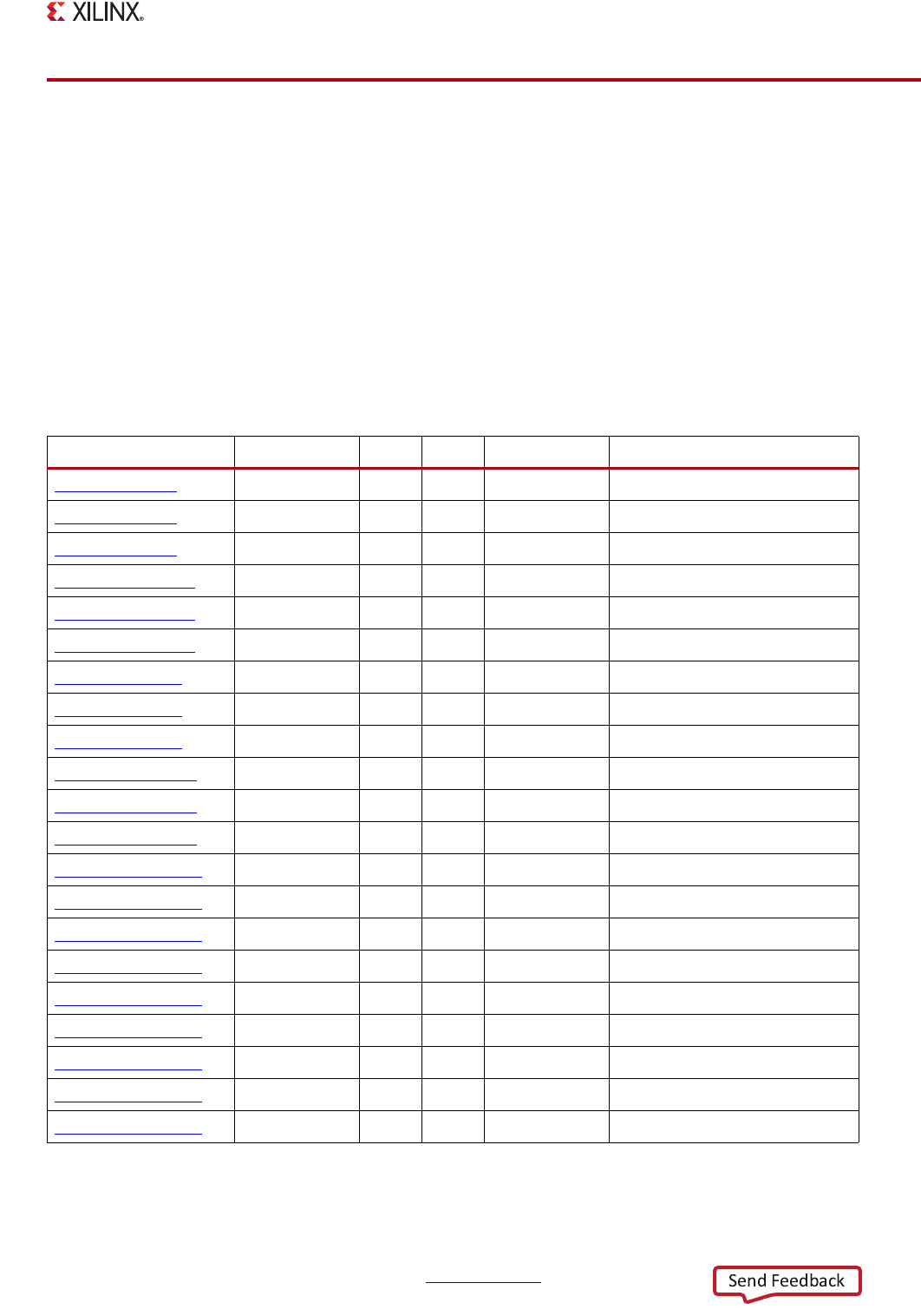
Register Summary
Module Name Triple Timer Counter (ttc)
Software Name XTTCPS
Base Address 0xF8001000 ttc0
0xF8002000 ttc1
Description Triple Timer Counter
Vendor Info
Register Name Address Width Type Reset Value Description
Clock_Control_1
0x00000000 7 rw 0x00000000 Clock Control register
Clock_Control_2
0x00000004 7 rw 0x00000000 Clock Control register
Clock_Control_3
0x00000008 7 rw 0x00000000 Clock Control register
Counter_Control_1
0x0000000C 7 rw 0x00000021 Operational mode and reset
Counter_Control_2
0x00000010 7 rw 0x00000021 Operational mode and reset
Counter_Control_3
0x00000014 7 rw 0x00000021 Operational mode and reset
Counter_Value_1
0x00000018 16 ro 0x00000000 Current counter value
Counter_Value_2
0x0000001C 16 ro 0x00000000 Current counter value
Counter_Value_3
0x00000020 16 ro 0x00000000 Current counter value
Interval_Counter_1
0x00000024 16 rw 0x00000000 Interval value
Interval_Counter_2
0x00000028 16 rw 0x00000000 Interval value
Interval_Counter_3
0x0000002C 16 rw 0x00000000 Interval value
Match_1_Counter_1
0x00000030 16 rw 0x00000000 Match value
Match_1_Counter_2
0x00000034 16 rw 0x00000000 Match value
Match_1_Counter_3
0x00000038 16 rw 0x00000000 Match value
Match_2_Counter_1
0x0000003C 16 rw 0x00000000 Match value
Match_2_Counter_2
0x00000040 16 rw 0x00000000 Match value
Match_2_Counter_3
0x00000044 16 rw 0x00000000 Match value
Match_3_Counter_1
0x00000048 16 rw 0x00000000 Match value
Match_3_Counter_2
0x0000004C 16 rw 0x00000000 Match value
Match_3_Counter_3
0x00000050 16 rw 0x00000000 Match value