
User manual


Table Of Contents
- Zynq-7000 All Programmable SoC
- Table of Contents
- Ch. 1: Introduction
- Ch. 2: Signals, Interfaces, and Pins
- Ch. 3: Application Processing Unit
- Ch. 4: System Addresses
- Ch. 5: Interconnect
- Ch. 6: Boot and Configuration
- Ch. 7: Interrupts
- Ch. 8: Timers
- Ch. 9: DMA Controller
- Introduction
- Functional Description
- DMA Transfers on the AXI Interconnect
- AXI Transaction Considerations
- DMA Manager
- Multi-channel Data FIFO (MFIFO)
- Memory-to-Memory Transfers
- PL Peripheral AXI Transactions
- PL Peripheral Request Interface
- PL Peripheral - Length Managed by PL Peripheral
- PL Peripheral - Length Managed by DMAC
- Events and Interrupts
- Aborts
- Security
- IP Configuration Options
- Programming Guide for DMA Controller
- Programming Guide for DMA Engine
- Programming Restrictions
- System Functions
- I/O Interface
- Ch. 10: DDR Memory Controller
- Introduction
- AXI Memory Port Interface (DDRI)
- DDR Core and Transaction Scheduler (DDRC)
- DDRC Arbitration
- Controller PHY (DDRP)
- Initialization and Calibration
- DDR Clock Initialization
- DDR IOB Impedance Calibration
- DDR IOB Configuration
- DDR Controller Register Programming
- DRAM Reset and Initialization
- DRAM Input Impedance (ODT) Calibration
- DRAM Output Impedance (RON) Calibration
- DRAM Training
- Write Data Eye Adjustment
- Alternatives to Automatic DRAM Training
- DRAM Write Latency Restriction
- Register Overview
- Error Correction Code (ECC)
- Programming Model
- Ch. 11: Static Memory Controller
- Ch. 12: Quad-SPI Flash Controller
- Ch. 13: SD/SDIO Controller
- Ch. 14: General Purpose I/O (GPIO)
- Ch. 15: USB Host, Device, and OTG Controller
- Introduction
- Functional Description
- Programming Overview and Reference
- Device Mode Control
- Device Endpoint Data Structures
- Device Endpoint Packet Operational Model
- Device Endpoint Descriptor Reference
- Programming Guide for Device Controller
- Programming Guide for Device Endpoint Data Structures
- Host Mode Data Structures
- EHCI Implementation
- Host Data Structures Reference
- Programming Guide for Host Controller
- OTG Description and Reference
- System Functions
- I/O Interfaces
- Ch. 16: Gigabit Ethernet Controller
- Ch. 17: SPI Controller
- Ch. 18: CAN Controller
- Ch. 19: UART Controller
- Ch. 20: I2C Controller
- Ch. 21: Programmable Logic Description
- Ch. 22: Programmable Logic Design Guide
- Ch. 23: Programmable Logic Test and Debug
- Ch. 24: Power Management
- Ch. 25: Clocks
- Ch. 26: Reset System
- Ch. 27: JTAG and DAP Subsystem
- Ch. 28: System Test and Debug
- Ch. 29: On-Chip Memory (OCM)
- Ch. 30: XADC Interface
- Ch. 31: PCI Express
- Ch. 32: Device Secure Boot
- Appx. A: Additional Resources
- Appx. B: Register Details
- Overview
- Acronyms
- Module Summary
- AXI_HP Interface (AFI) (axi_hp)
- CAN Controller (can)
- DDR Memory Controller (ddrc)
- CoreSight Cross Trigger Interface (cti)
- Performance Monitor Unit (cortexa9_pmu)
- CoreSight Program Trace Macrocell (ptm)
- Debug Access Port (dap)
- CoreSight Embedded Trace Buffer (etb)
- PL Fabric Trace Monitor (ftm)
- CoreSight Trace Funnel (funnel)
- CoreSight Intstrumentation Trace Macrocell (itm)
- CoreSight Trace Packet Output (tpiu)
- Device Configuration Interface (devcfg)
- DMA Controller (dmac)
- Gigabit Ethernet Controller (GEM)
- General Purpose I/O (gpio)
- Interconnect QoS (qos301)
- NIC301 Address Region Control (nic301_addr_region_ctrl_registers)
- I2C Controller (IIC)
- L2 Cache (L2Cpl310)
- Application Processing Unit (mpcore)
- On-Chip Memory (ocm)
- Quad-SPI Flash Controller (qspi)
- SD Controller (sdio)
- System Level Control Registers (slcr)
- Static Memory Controller (pl353)
- SPI Controller (SPI)
- System Watchdog Timer (swdt)
- Triple Timer Counter (ttc)
- UART Controller (UART)
- USB Controller (usb)
Zynq-7000 AP SoC Technical Reference Manual www.xilinx.com 1790
UG585 (v1.11) September 27, 2016
Appendix B: Register Details
B.33 UART Controller (UART)
Register Summary
Register (UART
) Control_reg0
Module Name UART Controller (UART)
Software Name XUARTPS
Base Address 0xE0000000 uart0
0xE0001000 uart1
Description Universal Asynchronous Receiver Transmitter
Vendor Info Cadence UART
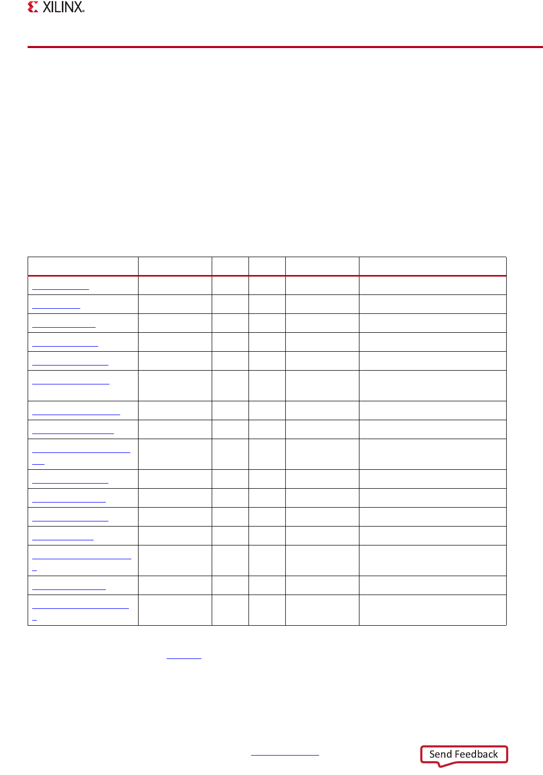
Register Name Address Width Type Reset Value Description
Control_reg0
0x00000000 32 mixed 0x00000128 UART Control Register
mode_reg0
0x00000004 32 mixed 0x00000000 UART Mode Register
Intrpt_en_reg0
0x00000008 32 mixed 0x00000000 Interrupt Enable Register
Intrpt_dis_reg0
0x0000000C 32 mixed 0x00000000 Interrupt Disable Register
Intrpt_mask_reg0
0x00000010 32 ro 0x00000000 Interrupt Mask Register
Chnl_int_sts_reg0
0x00000014 32 wtc 0x00000000 Channel Interrupt Status
Register
Baud_rate_gen_reg0
0x00000018 32 mixed 0x0000028B Baud Rate Generator Register.
Rcvr_timeout_reg0
0x0000001C 32 mixed 0x00000000 Receiver Timeout Register
Rcvr_FIFO_trigger_lev
el0
0x00000020 32 mixed 0x00000020 Receiver FIFO Trigger Level
Register
Modem_ctrl_reg0
0x00000024 32 mixed 0x00000000 Modem Control Register
Modem_sts_reg0
0x00000028 32 mixed x Modem Status Register
Channel_sts_reg0
0x0000002C 32 ro 0x00000000 Channel Status Register
TX_RX_FIFO0
0x00000030 32 mixed 0x00000000 Transmit and Receive FIFO
Baud_rate_divider_reg
0
0x00000034 32 mixed 0x0000000F Baud Rate Divider Register
Flow_delay_reg0
0x00000038 32 mixed 0x00000000 Flow Control Delay Register
Tx_FIFO_trigger_level
0
0x00000044 32 mixed 0x00000020 Transmitter FIFO Trigger Level
Register
Name Control_reg0