
User manual


Table Of Contents
- Zynq-7000 All Programmable SoC
- Table of Contents
- Ch. 1: Introduction
- Ch. 2: Signals, Interfaces, and Pins
- Ch. 3: Application Processing Unit
- Ch. 4: System Addresses
- Ch. 5: Interconnect
- Ch. 6: Boot and Configuration
- Ch. 7: Interrupts
- Ch. 8: Timers
- Ch. 9: DMA Controller
- Introduction
- Functional Description
- DMA Transfers on the AXI Interconnect
- AXI Transaction Considerations
- DMA Manager
- Multi-channel Data FIFO (MFIFO)
- Memory-to-Memory Transfers
- PL Peripheral AXI Transactions
- PL Peripheral Request Interface
- PL Peripheral - Length Managed by PL Peripheral
- PL Peripheral - Length Managed by DMAC
- Events and Interrupts
- Aborts
- Security
- IP Configuration Options
- Programming Guide for DMA Controller
- Programming Guide for DMA Engine
- Programming Restrictions
- System Functions
- I/O Interface
- Ch. 10: DDR Memory Controller
- Introduction
- AXI Memory Port Interface (DDRI)
- DDR Core and Transaction Scheduler (DDRC)
- DDRC Arbitration
- Controller PHY (DDRP)
- Initialization and Calibration
- DDR Clock Initialization
- DDR IOB Impedance Calibration
- DDR IOB Configuration
- DDR Controller Register Programming
- DRAM Reset and Initialization
- DRAM Input Impedance (ODT) Calibration
- DRAM Output Impedance (RON) Calibration
- DRAM Training
- Write Data Eye Adjustment
- Alternatives to Automatic DRAM Training
- DRAM Write Latency Restriction
- Register Overview
- Error Correction Code (ECC)
- Programming Model
- Ch. 11: Static Memory Controller
- Ch. 12: Quad-SPI Flash Controller
- Ch. 13: SD/SDIO Controller
- Ch. 14: General Purpose I/O (GPIO)
- Ch. 15: USB Host, Device, and OTG Controller
- Introduction
- Functional Description
- Programming Overview and Reference
- Device Mode Control
- Device Endpoint Data Structures
- Device Endpoint Packet Operational Model
- Device Endpoint Descriptor Reference
- Programming Guide for Device Controller
- Programming Guide for Device Endpoint Data Structures
- Host Mode Data Structures
- EHCI Implementation
- Host Data Structures Reference
- Programming Guide for Host Controller
- OTG Description and Reference
- System Functions
- I/O Interfaces
- Ch. 16: Gigabit Ethernet Controller
- Ch. 17: SPI Controller
- Ch. 18: CAN Controller
- Ch. 19: UART Controller
- Ch. 20: I2C Controller
- Ch. 21: Programmable Logic Description
- Ch. 22: Programmable Logic Design Guide
- Ch. 23: Programmable Logic Test and Debug
- Ch. 24: Power Management
- Ch. 25: Clocks
- Ch. 26: Reset System
- Ch. 27: JTAG and DAP Subsystem
- Ch. 28: System Test and Debug
- Ch. 29: On-Chip Memory (OCM)
- Ch. 30: XADC Interface
- Ch. 31: PCI Express
- Ch. 32: Device Secure Boot
- Appx. A: Additional Resources
- Appx. B: Register Details
- Overview
- Acronyms
- Module Summary
- AXI_HP Interface (AFI) (axi_hp)
- CAN Controller (can)
- DDR Memory Controller (ddrc)
- CoreSight Cross Trigger Interface (cti)
- Performance Monitor Unit (cortexa9_pmu)
- CoreSight Program Trace Macrocell (ptm)
- Debug Access Port (dap)
- CoreSight Embedded Trace Buffer (etb)
- PL Fabric Trace Monitor (ftm)
- CoreSight Trace Funnel (funnel)
- CoreSight Intstrumentation Trace Macrocell (itm)
- CoreSight Trace Packet Output (tpiu)
- Device Configuration Interface (devcfg)
- DMA Controller (dmac)
- Gigabit Ethernet Controller (GEM)
- General Purpose I/O (gpio)
- Interconnect QoS (qos301)
- NIC301 Address Region Control (nic301_addr_region_ctrl_registers)
- I2C Controller (IIC)
- L2 Cache (L2Cpl310)
- Application Processing Unit (mpcore)
- On-Chip Memory (ocm)
- Quad-SPI Flash Controller (qspi)
- SD Controller (sdio)
- System Level Control Registers (slcr)
- Static Memory Controller (pl353)
- SPI Controller (SPI)
- System Watchdog Timer (swdt)
- Triple Timer Counter (ttc)
- UART Controller (UART)
- USB Controller (usb)
Zynq-7000 AP SoC Technical Reference Manual www.xilinx.com 187
UG585 (v1.11) September 27, 2016
Chapter 6: Boot and Configuration
6.3.7 SD Card Boot
SD card boot supports these features:
• Boot from standard SD or SDHC cards
• FAT 16/32 file system
• Up to 32 GB card densities
Note: The SD card boot mode is not supported in 7z010 dual core and 7z007s single core CLG225
devices.
Note: The SD card boot mode does not support header search or multiboot.
BootROM Steps
The BootROM performs these steps in SD card boot mode:
1. Initializes the MIO pins listed in Table 6-15.
2. Configures SDIO_CLK_CTRL to a divisor of 32 and SD_CLK_CTL_R with a value of 1 (divide by 2).
3. Sets the SD controller to operate in 4-bit mode and use 3-byte addressing.
4. Tests the interface.
5. Reads BOOT.BIN from the root of the SD file system and copies it into OCM after parsing the
required BootROM Header.
6. BootROM transfer CPU execution to code downloaded into the OCM.
Note: Production devices do not test the Card Detection status. For preproduction devices, refer to
AR# 52016.
File Partitions
For the BootROM to read the BOOT.BIN file, the SD card must be partitioned so that the first
partition is a FAT 16/32 file system. Additional non-FAT partitions are permitted, but the BootROM
does not read the other partitions.
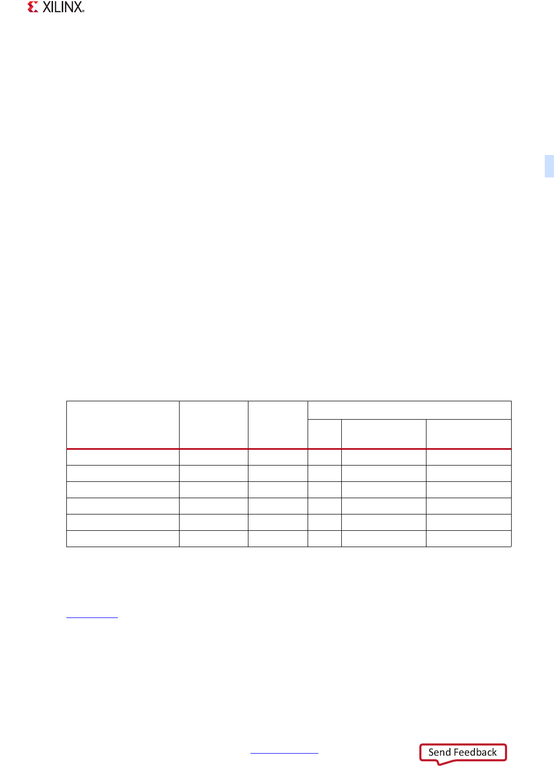
Table 6-15: SD Card Boot MIO Register Settings
SDIO
I/O Interface
Signal Name
MIO Pin
Number
MIO_PIN
Register
Setting
(1)
Pin State
I/O
I/O Buffer
Output, Pull-up
External
Connection
Not SD card boot MIO 0, 1 0x1601 I 3-state ~
Not SD card boot MIO 2 to 8 0x0601 I 3-state Pull-up/down
Not SD card boot MIO 9 to 39 0x1601 I 3-state ~
SDIO_0_CLK MIO 40 0x0680 OEnabled ~
SDIO_0_CMD MIO 41 0x0680 OEnabled ~
SDIO_0_DATA[0:3] MIO 42:45 0x1680 I/O Enabled, pull-up ~
Notes:
1. These register settings are for LVCMOS25/33. Change the 6 to a 2 for LVCMOS18 (bits 11:9 change from
011 to 001).