
User manual


Table Of Contents
- Zynq-7000 All Programmable SoC
- Table of Contents
- Ch. 1: Introduction
- Ch. 2: Signals, Interfaces, and Pins
- Ch. 3: Application Processing Unit
- Ch. 4: System Addresses
- Ch. 5: Interconnect
- Ch. 6: Boot and Configuration
- Ch. 7: Interrupts
- Ch. 8: Timers
- Ch. 9: DMA Controller
- Introduction
- Functional Description
- DMA Transfers on the AXI Interconnect
- AXI Transaction Considerations
- DMA Manager
- Multi-channel Data FIFO (MFIFO)
- Memory-to-Memory Transfers
- PL Peripheral AXI Transactions
- PL Peripheral Request Interface
- PL Peripheral - Length Managed by PL Peripheral
- PL Peripheral - Length Managed by DMAC
- Events and Interrupts
- Aborts
- Security
- IP Configuration Options
- Programming Guide for DMA Controller
- Programming Guide for DMA Engine
- Programming Restrictions
- System Functions
- I/O Interface
- Ch. 10: DDR Memory Controller
- Introduction
- AXI Memory Port Interface (DDRI)
- DDR Core and Transaction Scheduler (DDRC)
- DDRC Arbitration
- Controller PHY (DDRP)
- Initialization and Calibration
- DDR Clock Initialization
- DDR IOB Impedance Calibration
- DDR IOB Configuration
- DDR Controller Register Programming
- DRAM Reset and Initialization
- DRAM Input Impedance (ODT) Calibration
- DRAM Output Impedance (RON) Calibration
- DRAM Training
- Write Data Eye Adjustment
- Alternatives to Automatic DRAM Training
- DRAM Write Latency Restriction
- Register Overview
- Error Correction Code (ECC)
- Programming Model
- Ch. 11: Static Memory Controller
- Ch. 12: Quad-SPI Flash Controller
- Ch. 13: SD/SDIO Controller
- Ch. 14: General Purpose I/O (GPIO)
- Ch. 15: USB Host, Device, and OTG Controller
- Introduction
- Functional Description
- Programming Overview and Reference
- Device Mode Control
- Device Endpoint Data Structures
- Device Endpoint Packet Operational Model
- Device Endpoint Descriptor Reference
- Programming Guide for Device Controller
- Programming Guide for Device Endpoint Data Structures
- Host Mode Data Structures
- EHCI Implementation
- Host Data Structures Reference
- Programming Guide for Host Controller
- OTG Description and Reference
- System Functions
- I/O Interfaces
- Ch. 16: Gigabit Ethernet Controller
- Ch. 17: SPI Controller
- Ch. 18: CAN Controller
- Ch. 19: UART Controller
- Ch. 20: I2C Controller
- Ch. 21: Programmable Logic Description
- Ch. 22: Programmable Logic Design Guide
- Ch. 23: Programmable Logic Test and Debug
- Ch. 24: Power Management
- Ch. 25: Clocks
- Ch. 26: Reset System
- Ch. 27: JTAG and DAP Subsystem
- Ch. 28: System Test and Debug
- Ch. 29: On-Chip Memory (OCM)
- Ch. 30: XADC Interface
- Ch. 31: PCI Express
- Ch. 32: Device Secure Boot
- Appx. A: Additional Resources
- Appx. B: Register Details
- Overview
- Acronyms
- Module Summary
- AXI_HP Interface (AFI) (axi_hp)
- CAN Controller (can)
- DDR Memory Controller (ddrc)
- CoreSight Cross Trigger Interface (cti)
- Performance Monitor Unit (cortexa9_pmu)
- CoreSight Program Trace Macrocell (ptm)
- Debug Access Port (dap)
- CoreSight Embedded Trace Buffer (etb)
- PL Fabric Trace Monitor (ftm)
- CoreSight Trace Funnel (funnel)
- CoreSight Intstrumentation Trace Macrocell (itm)
- CoreSight Trace Packet Output (tpiu)
- Device Configuration Interface (devcfg)
- DMA Controller (dmac)
- Gigabit Ethernet Controller (GEM)
- General Purpose I/O (gpio)
- Interconnect QoS (qos301)
- NIC301 Address Region Control (nic301_addr_region_ctrl_registers)
- I2C Controller (IIC)
- L2 Cache (L2Cpl310)
- Application Processing Unit (mpcore)
- On-Chip Memory (ocm)
- Quad-SPI Flash Controller (qspi)
- SD Controller (sdio)
- System Level Control Registers (slcr)
- Static Memory Controller (pl353)
- SPI Controller (SPI)
- System Watchdog Timer (swdt)
- Triple Timer Counter (ttc)
- UART Controller (UART)
- USB Controller (usb)
Zynq-7000 AP SoC Technical Reference Manual www.xilinx.com 203
UG585 (v1.11) September 27, 2016
Chapter 6: Boot and Configuration
If a failure occurs while booting in secure mode, the BootROM disables the AES unit, clears the OCM,
clears the PL, and halts the processor. JTAG is not enabled, consequently, the REBOOT_STATUS value
is not available to be read. Instead, the 16-bit error code is shown by toggling the INIT_B pin.
6.3.14 Registers Modified by the BootROM – Examples
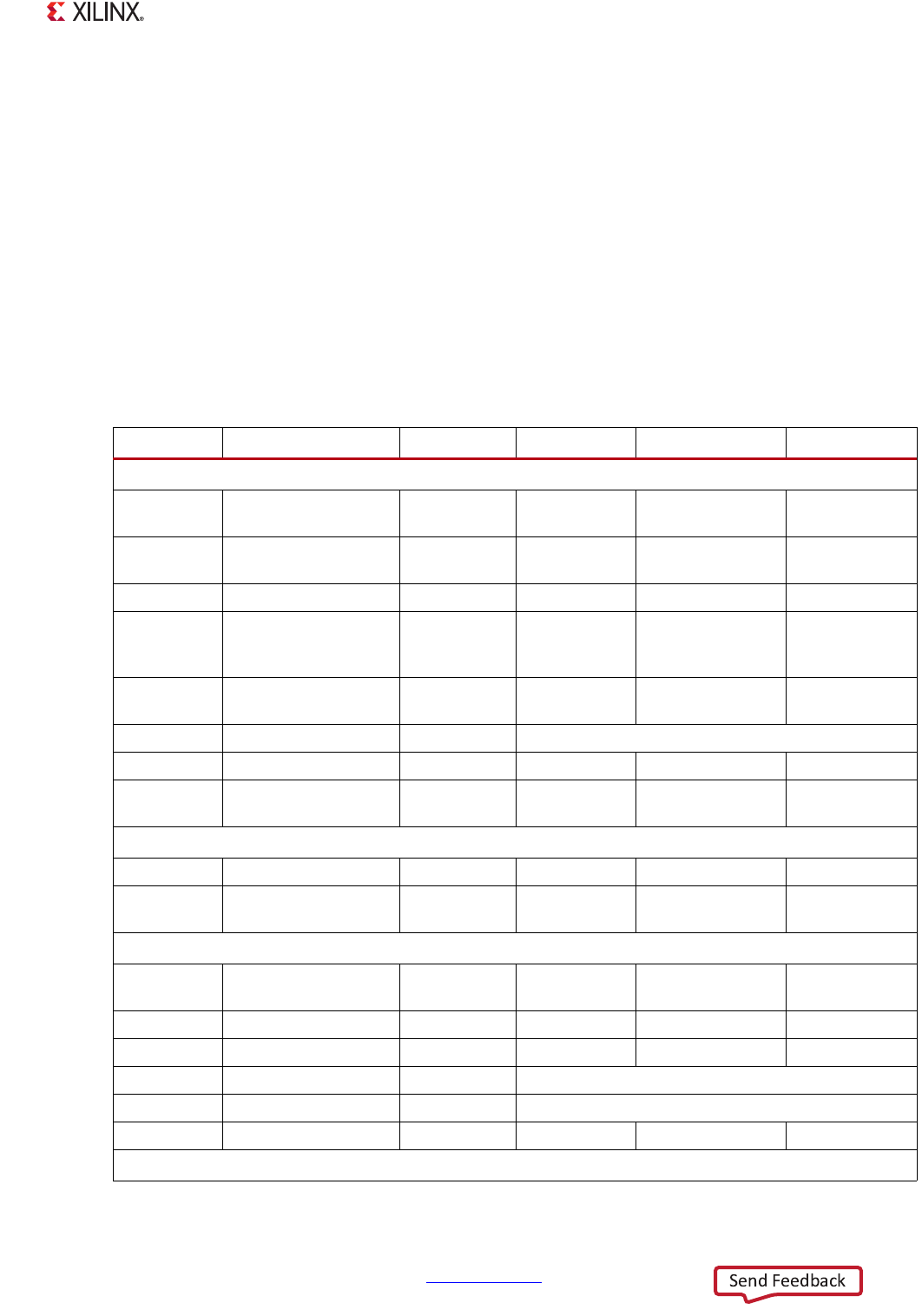
Examples of registers modified by the BootROM are listed in Table 6-22. When multiple register
values appear in the table, this indicates that the value depends on other factors. Refer to the
footnotes and text for more information. These are values that have been observed when the
BootROM transfers CPU control from the FSBL/User code.
These values were obtained from test run on the ZC702 board with the 7z020 production device and
the ZC706 board with the 7z035/7z045 production devices.
Table 6-22: BootROM Modified Registers
Address Register Name
(1)
Reset Value JTAG Boot Quad-SPI Boot SD Card Boot
devcfg Registers
0xF800_7000
CTRL
0x0C006000 0x4E00E07F
0x4C00E07F
0x4E80EE80
0x4E00E07F
0x4E80EE80
0xF800_7004
LOCK
0x00000000 0x0000001A
0x0000001A
0x00000012
0x0000001A
0x00000012
0xF800_7008
CFG
0x00000508 reset value reset value reset value
0xF800_700C
INT_STS
0x00000000
0xF8020006
0xA802000A
0xA802000B
0xA803000A
0xA803100A
0xA883100A
0xA802000A
0xA803000A
0xF800_7014
STATUS
0x40000820
0x40000F30
0x40000A30
0x40000A30 0x40000A30
0xF800_7028
ROM_SHADOW
0x00000000 0xFFFFFFFF
0xF800_7034
UNLOCK
0x00000000 0x757BDF0D 0x757BDF0D 0x757BDF0D
0xF800_7080
MCTRL
x
0x10800000
0x30800100
0x30800100 0x30800100
l2cache Registers
0xF8F0_2104
reg1_aux_control
0x02050000 0x02060000
0xF8F0_2F40
reg15_debug_ctrl
0x00000000 0x00000004
0x00000004
0x00000000
0x00000004
0x00000000
mpcore Registers
0xF8F0_0040
Filtering_Start_Addr
0x00100000
reset
value
reset value reset value
0xF8F0_0044
Filtering_End_Addr
0x00000000 0xFFE00000 0xFFE00000 0xFFE00000
0xF8F0_0108
ICCBPR
0x00000002 reset value
0xF8F0_0200
Global_Timer_Counter_0
0x00000000 The value depends on when the register is read.
0xF8F0_0204
Global_Timer_Counter_1
0x00000000 The value depends on when the register is read.
0xF8F0_0208
Global_Timer_Control
0x00000000 0x00000001 0x00000001
slcr Registers