
User manual


Table Of Contents
- Zynq-7000 All Programmable SoC
- Table of Contents
- Ch. 1: Introduction
- Ch. 2: Signals, Interfaces, and Pins
- Ch. 3: Application Processing Unit
- Ch. 4: System Addresses
- Ch. 5: Interconnect
- Ch. 6: Boot and Configuration
- Ch. 7: Interrupts
- Ch. 8: Timers
- Ch. 9: DMA Controller
- Introduction
- Functional Description
- DMA Transfers on the AXI Interconnect
- AXI Transaction Considerations
- DMA Manager
- Multi-channel Data FIFO (MFIFO)
- Memory-to-Memory Transfers
- PL Peripheral AXI Transactions
- PL Peripheral Request Interface
- PL Peripheral - Length Managed by PL Peripheral
- PL Peripheral - Length Managed by DMAC
- Events and Interrupts
- Aborts
- Security
- IP Configuration Options
- Programming Guide for DMA Controller
- Programming Guide for DMA Engine
- Programming Restrictions
- System Functions
- I/O Interface
- Ch. 10: DDR Memory Controller
- Introduction
- AXI Memory Port Interface (DDRI)
- DDR Core and Transaction Scheduler (DDRC)
- DDRC Arbitration
- Controller PHY (DDRP)
- Initialization and Calibration
- DDR Clock Initialization
- DDR IOB Impedance Calibration
- DDR IOB Configuration
- DDR Controller Register Programming
- DRAM Reset and Initialization
- DRAM Input Impedance (ODT) Calibration
- DRAM Output Impedance (RON) Calibration
- DRAM Training
- Write Data Eye Adjustment
- Alternatives to Automatic DRAM Training
- DRAM Write Latency Restriction
- Register Overview
- Error Correction Code (ECC)
- Programming Model
- Ch. 11: Static Memory Controller
- Ch. 12: Quad-SPI Flash Controller
- Ch. 13: SD/SDIO Controller
- Ch. 14: General Purpose I/O (GPIO)
- Ch. 15: USB Host, Device, and OTG Controller
- Introduction
- Functional Description
- Programming Overview and Reference
- Device Mode Control
- Device Endpoint Data Structures
- Device Endpoint Packet Operational Model
- Device Endpoint Descriptor Reference
- Programming Guide for Device Controller
- Programming Guide for Device Endpoint Data Structures
- Host Mode Data Structures
- EHCI Implementation
- Host Data Structures Reference
- Programming Guide for Host Controller
- OTG Description and Reference
- System Functions
- I/O Interfaces
- Ch. 16: Gigabit Ethernet Controller
- Ch. 17: SPI Controller
- Ch. 18: CAN Controller
- Ch. 19: UART Controller
- Ch. 20: I2C Controller
- Ch. 21: Programmable Logic Description
- Ch. 22: Programmable Logic Design Guide
- Ch. 23: Programmable Logic Test and Debug
- Ch. 24: Power Management
- Ch. 25: Clocks
- Ch. 26: Reset System
- Ch. 27: JTAG and DAP Subsystem
- Ch. 28: System Test and Debug
- Ch. 29: On-Chip Memory (OCM)
- Ch. 30: XADC Interface
- Ch. 31: PCI Express
- Ch. 32: Device Secure Boot
- Appx. A: Additional Resources
- Appx. B: Register Details
- Overview
- Acronyms
- Module Summary
- AXI_HP Interface (AFI) (axi_hp)
- CAN Controller (can)
- DDR Memory Controller (ddrc)
- CoreSight Cross Trigger Interface (cti)
- Performance Monitor Unit (cortexa9_pmu)
- CoreSight Program Trace Macrocell (ptm)
- Debug Access Port (dap)
- CoreSight Embedded Trace Buffer (etb)
- PL Fabric Trace Monitor (ftm)
- CoreSight Trace Funnel (funnel)
- CoreSight Intstrumentation Trace Macrocell (itm)
- CoreSight Trace Packet Output (tpiu)
- Device Configuration Interface (devcfg)
- DMA Controller (dmac)
- Gigabit Ethernet Controller (GEM)
- General Purpose I/O (gpio)
- Interconnect QoS (qos301)
- NIC301 Address Region Control (nic301_addr_region_ctrl_registers)
- I2C Controller (IIC)
- L2 Cache (L2Cpl310)
- Application Processing Unit (mpcore)
- On-Chip Memory (ocm)
- Quad-SPI Flash Controller (qspi)
- SD Controller (sdio)
- System Level Control Registers (slcr)
- Static Memory Controller (pl353)
- SPI Controller (SPI)
- System Watchdog Timer (swdt)
- Triple Timer Counter (ttc)
- UART Controller (UART)
- USB Controller (usb)
Zynq-7000 AP SoC Technical Reference Manual www.xilinx.com 204
UG585 (v1.11) September 27, 2016
Chapter 6: Boot and Configuration
6.4 Device Boot and PL Configuration
The Zynq device is a complex system that can be tightly controlled (secured) by the PS boot process
or be open and accessible in a friendly and/or development environment. The PS-centric control of
the Zynq device assumes a secure environment after a POR reset until the Encryption Status
parameter in the BootROM Header is read or until JTAG boot mode is detected. When security
discrepancies are detected, the BootROM executes a system lockdown.
Basic Boot Sequence
There are many different boot sequences. The common thread is that after a system reset (POR and
non-POR), the BootROM executes first to configure and control the system. After a POR reset, there
are a few hardware activities that are performed before the BootROM executes. These hardware
activities are described in Figure 6-1, page 150. After the BootROM executes, the FSBL/User code
takes control of the PS and is able to further configure the device, including the PL.
1. Power-up and Reset Operations. See section 6.2 Device Start-up.
2. BootROM Execution. See section 6.3.3 BootROM Performance.
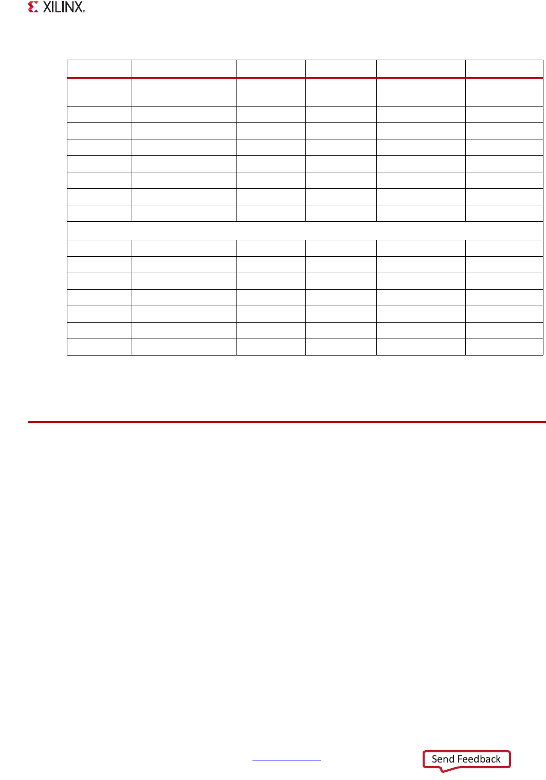
0xF800_0258
REBOOT_STATUS
(2)
0x00400000 0x00400002
0x00400000
0x00600000
0x00400000
0x00600000
0xF800_0910
OCM_CFG
0x00000000 0x00000018 0x00000018 0x00000018
0xF800_0A1C
Reserved
0x00010101 0x00010101 0x00020202 0x00020202
0xF800_0B04
GIOB_CFG_CMOS18
0x00000000 0x0C301166 0x0C301166 0x0C301166
0xF800_0B08
GIOB_CFG_CMOS25
0x00000000 0x0C301100 0x0C301100 0x0C301100
0xF800_0B0C
GIOB_CFG_CMOS33
0x00000000 0x0C301166 0x0C301166 0x0C301166
0xF800_0B14
GIOB_CFG_HSTL 0x00000000 0x0C750077 0x0C750077 0x0C750077
0xF800_0B70
DDRIOB_DCI_CTRL 0x00000020 reset value 0x00000823 0x00000823
uart1 Registers
0xE000_1000
Control_reg0
0x00000128 0x00000114 0x00000114 0x00000114
0xE000_1004
mode_reg0
0x00000000 0x00000020 0x00000020 0x00000020
0xE000_1014
Chnl_int_sts_reg0
0x00000200 reset value 0x00000E10 0x00000E10
0xE000_1018
Baud_rate_gen_reg0
0x0000028B reset value 0x0000003E 0x0000003E
0xE000_1028
Modem_sts_reg0
x 0x000000FB 0x000000FB 0x000000FB
0xE000_102C
Channel_sts_reg0
0x00000000 reset value 0x00006812 0x00006812
0xE000_1034
Baud_rate_divider
0x0000000F reset value 0x00000006 0x00000006
Notes:
1. Some register names are truncated or abbreviated to keep them short in this table.
2. In the REBOOT_STATUS register, a 4 means a POR reset and a 6 means an SRST (non-POR) reset.
Table 6-22: BootROM Modified Registers (Cont’d)
Address Register Name
(1)
Reset Value JTAG Boot Quad-SPI Boot SD Card Boot