
User manual


Table Of Contents
- Zynq-7000 All Programmable SoC
- Table of Contents
- Ch. 1: Introduction
- Ch. 2: Signals, Interfaces, and Pins
- Ch. 3: Application Processing Unit
- Ch. 4: System Addresses
- Ch. 5: Interconnect
- Ch. 6: Boot and Configuration
- Ch. 7: Interrupts
- Ch. 8: Timers
- Ch. 9: DMA Controller
- Introduction
- Functional Description
- DMA Transfers on the AXI Interconnect
- AXI Transaction Considerations
- DMA Manager
- Multi-channel Data FIFO (MFIFO)
- Memory-to-Memory Transfers
- PL Peripheral AXI Transactions
- PL Peripheral Request Interface
- PL Peripheral - Length Managed by PL Peripheral
- PL Peripheral - Length Managed by DMAC
- Events and Interrupts
- Aborts
- Security
- IP Configuration Options
- Programming Guide for DMA Controller
- Programming Guide for DMA Engine
- Programming Restrictions
- System Functions
- I/O Interface
- Ch. 10: DDR Memory Controller
- Introduction
- AXI Memory Port Interface (DDRI)
- DDR Core and Transaction Scheduler (DDRC)
- DDRC Arbitration
- Controller PHY (DDRP)
- Initialization and Calibration
- DDR Clock Initialization
- DDR IOB Impedance Calibration
- DDR IOB Configuration
- DDR Controller Register Programming
- DRAM Reset and Initialization
- DRAM Input Impedance (ODT) Calibration
- DRAM Output Impedance (RON) Calibration
- DRAM Training
- Write Data Eye Adjustment
- Alternatives to Automatic DRAM Training
- DRAM Write Latency Restriction
- Register Overview
- Error Correction Code (ECC)
- Programming Model
- Ch. 11: Static Memory Controller
- Ch. 12: Quad-SPI Flash Controller
- Ch. 13: SD/SDIO Controller
- Ch. 14: General Purpose I/O (GPIO)
- Ch. 15: USB Host, Device, and OTG Controller
- Introduction
- Functional Description
- Programming Overview and Reference
- Device Mode Control
- Device Endpoint Data Structures
- Device Endpoint Packet Operational Model
- Device Endpoint Descriptor Reference
- Programming Guide for Device Controller
- Programming Guide for Device Endpoint Data Structures
- Host Mode Data Structures
- EHCI Implementation
- Host Data Structures Reference
- Programming Guide for Host Controller
- OTG Description and Reference
- System Functions
- I/O Interfaces
- Ch. 16: Gigabit Ethernet Controller
- Ch. 17: SPI Controller
- Ch. 18: CAN Controller
- Ch. 19: UART Controller
- Ch. 20: I2C Controller
- Ch. 21: Programmable Logic Description
- Ch. 22: Programmable Logic Design Guide
- Ch. 23: Programmable Logic Test and Debug
- Ch. 24: Power Management
- Ch. 25: Clocks
- Ch. 26: Reset System
- Ch. 27: JTAG and DAP Subsystem
- Ch. 28: System Test and Debug
- Ch. 29: On-Chip Memory (OCM)
- Ch. 30: XADC Interface
- Ch. 31: PCI Express
- Ch. 32: Device Secure Boot
- Appx. A: Additional Resources
- Appx. B: Register Details
- Overview
- Acronyms
- Module Summary
- AXI_HP Interface (AFI) (axi_hp)
- CAN Controller (can)
- DDR Memory Controller (ddrc)
- CoreSight Cross Trigger Interface (cti)
- Performance Monitor Unit (cortexa9_pmu)
- CoreSight Program Trace Macrocell (ptm)
- Debug Access Port (dap)
- CoreSight Embedded Trace Buffer (etb)
- PL Fabric Trace Monitor (ftm)
- CoreSight Trace Funnel (funnel)
- CoreSight Intstrumentation Trace Macrocell (itm)
- CoreSight Trace Packet Output (tpiu)
- Device Configuration Interface (devcfg)
- DMA Controller (dmac)
- Gigabit Ethernet Controller (GEM)
- General Purpose I/O (gpio)
- Interconnect QoS (qos301)
- NIC301 Address Region Control (nic301_addr_region_ctrl_registers)
- I2C Controller (IIC)
- L2 Cache (L2Cpl310)
- Application Processing Unit (mpcore)
- On-Chip Memory (ocm)
- Quad-SPI Flash Controller (qspi)
- SD Controller (sdio)
- System Level Control Registers (slcr)
- Static Memory Controller (pl353)
- SPI Controller (SPI)
- System Watchdog Timer (swdt)
- Triple Timer Counter (ttc)
- UART Controller (UART)
- USB Controller (usb)
Zynq-7000 AP SoC Technical Reference Manual www.xilinx.com 207
UG585 (v1.11) September 27, 2016
Chapter 6: Boot and Configuration
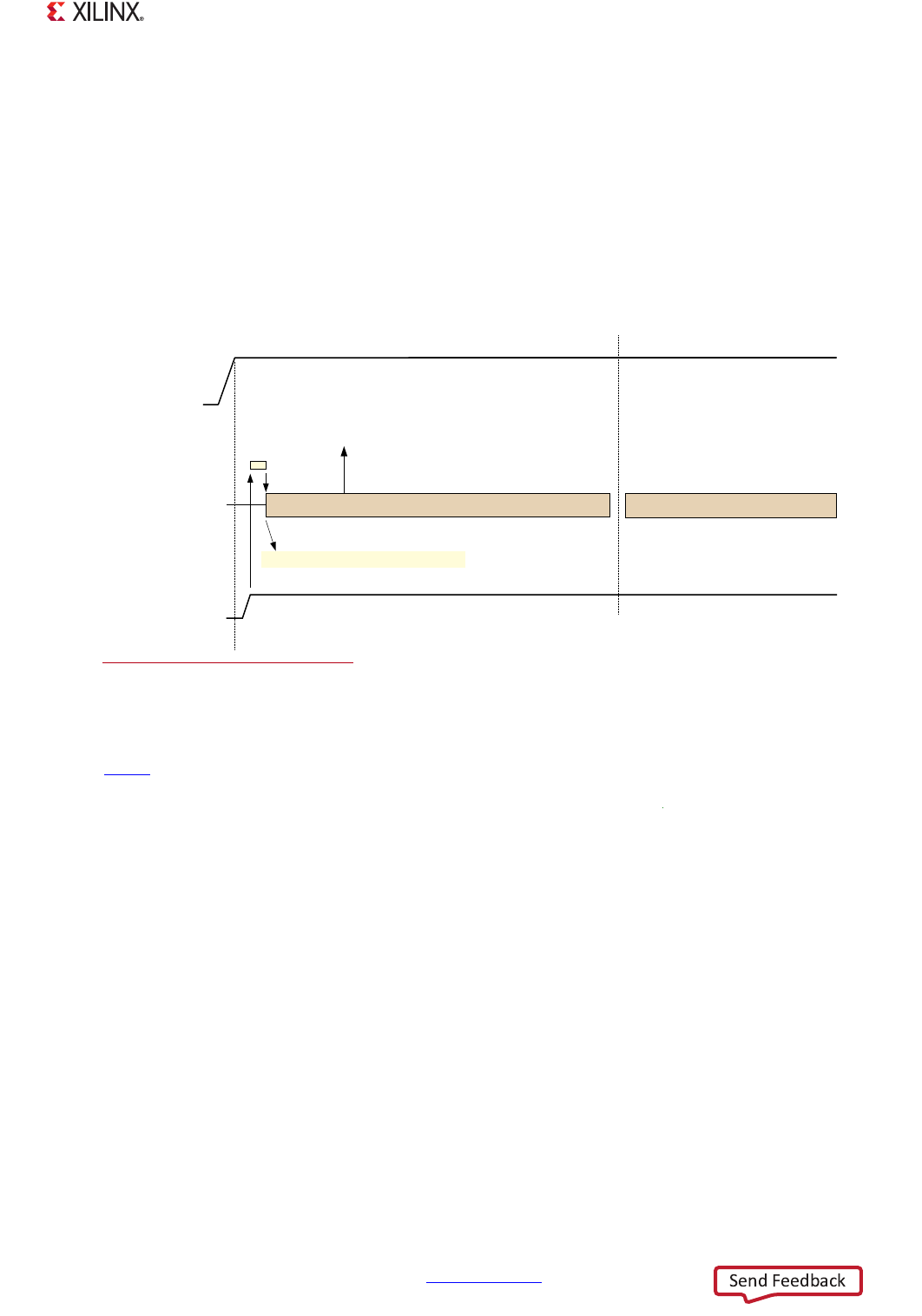
PS Non-secure Bring-up Example
The PS and PL can be brought up together in a secure or non-secure mode. The simultaneous
bring-up of the PS and PL is shown in Figure 6-12. Also refer to Figure 6-4, page 163 for details on
power, reset, and clock interactions and timing examples.The PS non-secure bring-up using a flash
device without JTAG illustrates a simple example with minimal resources. The example is shown in
Figure 6-14. When the PL is needed later in the system operation, its bring-up is explained in the PL
Bring-up by FSBL/User Code example.
PS Bring-up with PL Configuration Example
The PS and PL can be brought up together in a secure or non-secure mode. The simultaneous
bring-up of the PS and PL is shown in Figure 6-15. Also refer to Figure 6-4, page 163 for details on
power, reset, and clock interactions and timing examples.
In this example, the bring-up process boots from a flash memory device. The BootROM supports
both secure (encrypted images) and non-secure boot modes (no encryption). This bring-up
sequence is summarized in these steps below. The non-secure boot without the PL is illustrated in
Figure 6-14 and the secure boot mode with PL is illustrated in Figure 6-15:
1. Power-supplies are stable, PS_CLK is stable. See section 6.2.3 Clocks and PLLs.
2. PS_POR_B reset deasserts; for Secure boot, the PL is powered-on with the PS and self initializes.
3. BootROM executes in CPU 0:
a. Reads slcr.BOOT_MODE register to determine boot device.
X-Ref Target - Figure 6-13
X-Ref Target - Figure 6-14
Figure 6-14: PS Non-secure Bring-up Example
1) PLL lock time. The PLL lock time is discussed in section 6.3.3 BootROM Performance.
2) BootROM Execution. This time is highly dependent on the bandwidth of the flash device interface. For BootROM
execution, refer to section 6.3.3 BootROM Performance.
3) FSBL/User Code Execution. The execution time for the FSBL/User code is beyond the scope of UG585, please refer to
UG821, Zynq-7000 All Programmable SoC Software Developers Guide.
8*BFBB
6HTXHQFH
361RQVHFXUH%ULQJXS
36B325B%
)6%/8VHU&RGH([HFXWHV
36&38
%RRW520([HFXWHVDIWHUWKH3//VORFN
%RRW520([HFXWHV
WRPVVHHQRWH
%RRW5200RYHV
)6%/8VHU&RGHWR2&00HPRU\
6HHQRWH
36
3RZHURQ
3///RFN
XV
6HHQRWH