
User manual


Table Of Contents
- Zynq-7000 All Programmable SoC
- Table of Contents
- Ch. 1: Introduction
- Ch. 2: Signals, Interfaces, and Pins
- Ch. 3: Application Processing Unit
- Ch. 4: System Addresses
- Ch. 5: Interconnect
- Ch. 6: Boot and Configuration
- Ch. 7: Interrupts
- Ch. 8: Timers
- Ch. 9: DMA Controller
- Introduction
- Functional Description
- DMA Transfers on the AXI Interconnect
- AXI Transaction Considerations
- DMA Manager
- Multi-channel Data FIFO (MFIFO)
- Memory-to-Memory Transfers
- PL Peripheral AXI Transactions
- PL Peripheral Request Interface
- PL Peripheral - Length Managed by PL Peripheral
- PL Peripheral - Length Managed by DMAC
- Events and Interrupts
- Aborts
- Security
- IP Configuration Options
- Programming Guide for DMA Controller
- Programming Guide for DMA Engine
- Programming Restrictions
- System Functions
- I/O Interface
- Ch. 10: DDR Memory Controller
- Introduction
- AXI Memory Port Interface (DDRI)
- DDR Core and Transaction Scheduler (DDRC)
- DDRC Arbitration
- Controller PHY (DDRP)
- Initialization and Calibration
- DDR Clock Initialization
- DDR IOB Impedance Calibration
- DDR IOB Configuration
- DDR Controller Register Programming
- DRAM Reset and Initialization
- DRAM Input Impedance (ODT) Calibration
- DRAM Output Impedance (RON) Calibration
- DRAM Training
- Write Data Eye Adjustment
- Alternatives to Automatic DRAM Training
- DRAM Write Latency Restriction
- Register Overview
- Error Correction Code (ECC)
- Programming Model
- Ch. 11: Static Memory Controller
- Ch. 12: Quad-SPI Flash Controller
- Ch. 13: SD/SDIO Controller
- Ch. 14: General Purpose I/O (GPIO)
- Ch. 15: USB Host, Device, and OTG Controller
- Introduction
- Functional Description
- Programming Overview and Reference
- Device Mode Control
- Device Endpoint Data Structures
- Device Endpoint Packet Operational Model
- Device Endpoint Descriptor Reference
- Programming Guide for Device Controller
- Programming Guide for Device Endpoint Data Structures
- Host Mode Data Structures
- EHCI Implementation
- Host Data Structures Reference
- Programming Guide for Host Controller
- OTG Description and Reference
- System Functions
- I/O Interfaces
- Ch. 16: Gigabit Ethernet Controller
- Ch. 17: SPI Controller
- Ch. 18: CAN Controller
- Ch. 19: UART Controller
- Ch. 20: I2C Controller
- Ch. 21: Programmable Logic Description
- Ch. 22: Programmable Logic Design Guide
- Ch. 23: Programmable Logic Test and Debug
- Ch. 24: Power Management
- Ch. 25: Clocks
- Ch. 26: Reset System
- Ch. 27: JTAG and DAP Subsystem
- Ch. 28: System Test and Debug
- Ch. 29: On-Chip Memory (OCM)
- Ch. 30: XADC Interface
- Ch. 31: PCI Express
- Ch. 32: Device Secure Boot
- Appx. A: Additional Resources
- Appx. B: Register Details
- Overview
- Acronyms
- Module Summary
- AXI_HP Interface (AFI) (axi_hp)
- CAN Controller (can)
- DDR Memory Controller (ddrc)
- CoreSight Cross Trigger Interface (cti)
- Performance Monitor Unit (cortexa9_pmu)
- CoreSight Program Trace Macrocell (ptm)
- Debug Access Port (dap)
- CoreSight Embedded Trace Buffer (etb)
- PL Fabric Trace Monitor (ftm)
- CoreSight Trace Funnel (funnel)
- CoreSight Intstrumentation Trace Macrocell (itm)
- CoreSight Trace Packet Output (tpiu)
- Device Configuration Interface (devcfg)
- DMA Controller (dmac)
- Gigabit Ethernet Controller (GEM)
- General Purpose I/O (gpio)
- Interconnect QoS (qos301)
- NIC301 Address Region Control (nic301_addr_region_ctrl_registers)
- I2C Controller (IIC)
- L2 Cache (L2Cpl310)
- Application Processing Unit (mpcore)
- On-Chip Memory (ocm)
- Quad-SPI Flash Controller (qspi)
- SD Controller (sdio)
- System Level Control Registers (slcr)
- Static Memory Controller (pl353)
- SPI Controller (SPI)
- System Watchdog Timer (swdt)
- Triple Timer Counter (ttc)
- UART Controller (UART)
- USB Controller (usb)
Zynq-7000 AP SoC Technical Reference Manual www.xilinx.com 209
UG585 (v1.11) September 27, 2016
Chapter 6: Boot and Configuration
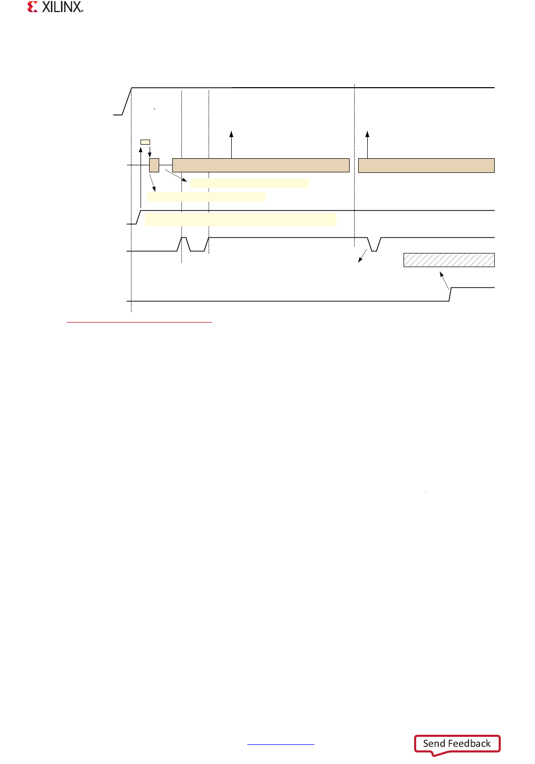
PL Bring-up by FSBL/User Code Example
The PL may not be initially initialized and configured after a device boot. The PL may also be shut
down during system operation. This example illustrates how the PL can be configured from scratch
under the control the FSBL/User code.
X-Ref Target - Figure 6-15
Figure 6-15: PS Bring-up with PL Configuration Option Example
1) PL T
POR
and PLL Lock Time. The T
POR
time is dependent on the voltage ramp of the power supply and is defined in
the data sheet. If the PL is already powered-up, then T
POR
time = 0. The PLL Lock time is specified in the data sheet
with the T
LOCK_PSPLL
parameter. The PLL is locked before the BootROM starts to execute.
2) PL Init Time. This happens very quickly and is affected by the size of the PL.
3) BootROM Decrypts FSLB/User Code. The BootROM copies the encrypted boot image to OCM memory. The DevC
DMA controller reads the image into its RxFIFO, sends it through the AES or HMAC units, and then writes the image
back to OCM memory. The time depends on many factors: type of Flash device interface, PS_CLK frequency and the
image size. This time range is taken from Table 6-8, page 178.
4) FSBL/User Code Configures PL. The PS software programs the DMA to read the bitstream and optionally decrypt it
before going to the PL Configuration module. The time depends on many factors: type of Flash device interface,
PS_CLK frequency, bitstream size, and if the bitstream is encrypted.
5) Enable PL. After the PL is configured, the [PCFG_DONE_INT] bit asserts and the user code enables the voltage level
shifters. A power-up sequence example is shown in section 2.4 PS–PL Voltage Level Shifter Enables.
8*BFBDB
,1,7B%
2'2XWSXW
'21(
2'2XWSXW
%RRW520,QLWLDOL]HG3/IRUHQFU\SWHG
FRGHWRJJOHV>3&)*B352*B%@ELW
3/LV
&RQILJXUHG
36B325B%
)6%/8VHU&RGH([HFXWHV
36&38
6HOIWLPHG
%RRW520([HFXWHVDIWHUWKH3//VORFN
%RRW520([HFXWHV
3/
,QLW
>3&)*B'21(B,17@
5HDG
6HTXHQFH
36%ULQJXSZLWK3/&RQILJXUDWLRQ2SWLRQ
QRWH
WRPVVHHQRWH
3/
7
325
WRPV
QRWH
7KH3/LVLQDFFHVVLEOHWRWKHXVHUIURP36B325B%UHVHWGHDVVHUWLRQ
XQWLOLWLVHQDEOHGE\WKH%RRW520
%RRW520'HFU\SWV
)6%/8VHU&RGH
)6%/,QLWLDOL]HG3/SULRU
WR&RQILJXUDWLRQWRJJOHV
>3&)*B352*B%@ELW
6HHQRWH
363/
3RZHURQ
3///RFN
XV
)6%/8VHU&RGH
&RQILJXUHV3/
%RRW520ZDLWVIRU3/7325
127()LJXUHQRWWRVFDOH
WRPV