
User manual


Table Of Contents
- Zynq-7000 All Programmable SoC
- Table of Contents
- Ch. 1: Introduction
- Ch. 2: Signals, Interfaces, and Pins
- Ch. 3: Application Processing Unit
- Ch. 4: System Addresses
- Ch. 5: Interconnect
- Ch. 6: Boot and Configuration
- Ch. 7: Interrupts
- Ch. 8: Timers
- Ch. 9: DMA Controller
- Introduction
- Functional Description
- DMA Transfers on the AXI Interconnect
- AXI Transaction Considerations
- DMA Manager
- Multi-channel Data FIFO (MFIFO)
- Memory-to-Memory Transfers
- PL Peripheral AXI Transactions
- PL Peripheral Request Interface
- PL Peripheral - Length Managed by PL Peripheral
- PL Peripheral - Length Managed by DMAC
- Events and Interrupts
- Aborts
- Security
- IP Configuration Options
- Programming Guide for DMA Controller
- Programming Guide for DMA Engine
- Programming Restrictions
- System Functions
- I/O Interface
- Ch. 10: DDR Memory Controller
- Introduction
- AXI Memory Port Interface (DDRI)
- DDR Core and Transaction Scheduler (DDRC)
- DDRC Arbitration
- Controller PHY (DDRP)
- Initialization and Calibration
- DDR Clock Initialization
- DDR IOB Impedance Calibration
- DDR IOB Configuration
- DDR Controller Register Programming
- DRAM Reset and Initialization
- DRAM Input Impedance (ODT) Calibration
- DRAM Output Impedance (RON) Calibration
- DRAM Training
- Write Data Eye Adjustment
- Alternatives to Automatic DRAM Training
- DRAM Write Latency Restriction
- Register Overview
- Error Correction Code (ECC)
- Programming Model
- Ch. 11: Static Memory Controller
- Ch. 12: Quad-SPI Flash Controller
- Ch. 13: SD/SDIO Controller
- Ch. 14: General Purpose I/O (GPIO)
- Ch. 15: USB Host, Device, and OTG Controller
- Introduction
- Functional Description
- Programming Overview and Reference
- Device Mode Control
- Device Endpoint Data Structures
- Device Endpoint Packet Operational Model
- Device Endpoint Descriptor Reference
- Programming Guide for Device Controller
- Programming Guide for Device Endpoint Data Structures
- Host Mode Data Structures
- EHCI Implementation
- Host Data Structures Reference
- Programming Guide for Host Controller
- OTG Description and Reference
- System Functions
- I/O Interfaces
- Ch. 16: Gigabit Ethernet Controller
- Ch. 17: SPI Controller
- Ch. 18: CAN Controller
- Ch. 19: UART Controller
- Ch. 20: I2C Controller
- Ch. 21: Programmable Logic Description
- Ch. 22: Programmable Logic Design Guide
- Ch. 23: Programmable Logic Test and Debug
- Ch. 24: Power Management
- Ch. 25: Clocks
- Ch. 26: Reset System
- Ch. 27: JTAG and DAP Subsystem
- Ch. 28: System Test and Debug
- Ch. 29: On-Chip Memory (OCM)
- Ch. 30: XADC Interface
- Ch. 31: PCI Express
- Ch. 32: Device Secure Boot
- Appx. A: Additional Resources
- Appx. B: Register Details
- Overview
- Acronyms
- Module Summary
- AXI_HP Interface (AFI) (axi_hp)
- CAN Controller (can)
- DDR Memory Controller (ddrc)
- CoreSight Cross Trigger Interface (cti)
- Performance Monitor Unit (cortexa9_pmu)
- CoreSight Program Trace Macrocell (ptm)
- Debug Access Port (dap)
- CoreSight Embedded Trace Buffer (etb)
- PL Fabric Trace Monitor (ftm)
- CoreSight Trace Funnel (funnel)
- CoreSight Intstrumentation Trace Macrocell (itm)
- CoreSight Trace Packet Output (tpiu)
- Device Configuration Interface (devcfg)
- DMA Controller (dmac)
- Gigabit Ethernet Controller (GEM)
- General Purpose I/O (gpio)
- Interconnect QoS (qos301)
- NIC301 Address Region Control (nic301_addr_region_ctrl_registers)
- I2C Controller (IIC)
- L2 Cache (L2Cpl310)
- Application Processing Unit (mpcore)
- On-Chip Memory (ocm)
- Quad-SPI Flash Controller (qspi)
- SD Controller (sdio)
- System Level Control Registers (slcr)
- Static Memory Controller (pl353)
- SPI Controller (SPI)
- System Watchdog Timer (swdt)
- Triple Timer Counter (ttc)
- UART Controller (UART)
- USB Controller (usb)
Zynq-7000 AP SoC Technical Reference Manual www.xilinx.com 212
UG585 (v1.11) September 27, 2016
Chapter 6: Boot and Configuration
The bridge supports both concurrent (bidirectional) and non-concurrent (unidirectional) download
and upload of boot images. Transmit and receive FIFOs buffer data between the PS AXI Interconnect
and the PCAP interface. For PCAP data, the bridge converts 32-bit AXI formatted data to the 32-bit
PCAP protocol and vice versa.
Non-secure bitstreams and boot images sent to the PCAP interface can be sent every PCAP clock
cycle. Secure (encrypted) data is sent to the PCAP interface every four PCAP clock cycles.
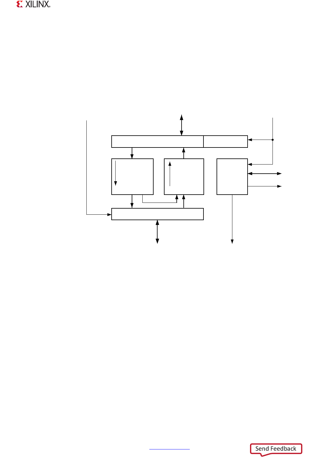
The architecture of the PCAP bridge is shown in Figure 6-17.
The PL must be powered on to use the DevC module, including the PCAP bridge and PCAP
configuration module. The PCAP interface is enabled by setting the devcfg.CTRL [PCAP_MODE] and
[PCAP_PR] bits = 1 as illustrated in Figure 6-2, page 157. If encrypted bitstreams or boot images are
being sent, then the devcfg.CTRL [QUARTER_PCAP_RATE_EN] bit must be set = 1 to match the 32-bit
PCAP interface to the 8-bit AES/HMAC unit interface.
To start a DMA transfer, these four DMA registers must be written in this order:
1. Source Address register, devcfg.DMA_SRC_ADDR
2. Destination Address register, devcfg.DMA_DST_ADDR
3. Source Length register, devcfg.DMA_SRC_LEN
4. Destination Length register, devcfg.DMA_DEST_LEN (triggers DMA transfer)
In all modes, the DMA transactions must be 64-byte aligned to prevent accidently crossing a 4K byte
boundary. The DMA status is tracked using the devcfg.INT_STS [DMA_DONE_INT] and
[D_P_DONE_INT] bits. They can be monitored using either interrupts or a polling method.
X-Ref Target - Figure 6-17
Figure 6-17: PCAP Bridge Architecture
3&$3&RQWURO
8*BFBB
$;,0DVWHU,QWHUIDFH
36$;,,QWHUFRQQHFW
'0$&RQWUROOHU
7UDQVPLWWHU
),)2
5HFHLYHU
),)2
&RQWURODQG
6WDWXV
5HJLVWHUV
&38B[FORFN
3&$3,QWHUIDFH
$3%
XSORDGGRZQORDG
3/3&$3
3&$3FORFN
,54
/RRSEDFN