
User manual


Table Of Contents
- Zynq-7000 All Programmable SoC
- Table of Contents
- Ch. 1: Introduction
- Ch. 2: Signals, Interfaces, and Pins
- Ch. 3: Application Processing Unit
- Ch. 4: System Addresses
- Ch. 5: Interconnect
- Ch. 6: Boot and Configuration
- Ch. 7: Interrupts
- Ch. 8: Timers
- Ch. 9: DMA Controller
- Introduction
- Functional Description
- DMA Transfers on the AXI Interconnect
- AXI Transaction Considerations
- DMA Manager
- Multi-channel Data FIFO (MFIFO)
- Memory-to-Memory Transfers
- PL Peripheral AXI Transactions
- PL Peripheral Request Interface
- PL Peripheral - Length Managed by PL Peripheral
- PL Peripheral - Length Managed by DMAC
- Events and Interrupts
- Aborts
- Security
- IP Configuration Options
- Programming Guide for DMA Controller
- Programming Guide for DMA Engine
- Programming Restrictions
- System Functions
- I/O Interface
- Ch. 10: DDR Memory Controller
- Introduction
- AXI Memory Port Interface (DDRI)
- DDR Core and Transaction Scheduler (DDRC)
- DDRC Arbitration
- Controller PHY (DDRP)
- Initialization and Calibration
- DDR Clock Initialization
- DDR IOB Impedance Calibration
- DDR IOB Configuration
- DDR Controller Register Programming
- DRAM Reset and Initialization
- DRAM Input Impedance (ODT) Calibration
- DRAM Output Impedance (RON) Calibration
- DRAM Training
- Write Data Eye Adjustment
- Alternatives to Automatic DRAM Training
- DRAM Write Latency Restriction
- Register Overview
- Error Correction Code (ECC)
- Programming Model
- Ch. 11: Static Memory Controller
- Ch. 12: Quad-SPI Flash Controller
- Ch. 13: SD/SDIO Controller
- Ch. 14: General Purpose I/O (GPIO)
- Ch. 15: USB Host, Device, and OTG Controller
- Introduction
- Functional Description
- Programming Overview and Reference
- Device Mode Control
- Device Endpoint Data Structures
- Device Endpoint Packet Operational Model
- Device Endpoint Descriptor Reference
- Programming Guide for Device Controller
- Programming Guide for Device Endpoint Data Structures
- Host Mode Data Structures
- EHCI Implementation
- Host Data Structures Reference
- Programming Guide for Host Controller
- OTG Description and Reference
- System Functions
- I/O Interfaces
- Ch. 16: Gigabit Ethernet Controller
- Ch. 17: SPI Controller
- Ch. 18: CAN Controller
- Ch. 19: UART Controller
- Ch. 20: I2C Controller
- Ch. 21: Programmable Logic Description
- Ch. 22: Programmable Logic Design Guide
- Ch. 23: Programmable Logic Test and Debug
- Ch. 24: Power Management
- Ch. 25: Clocks
- Ch. 26: Reset System
- Ch. 27: JTAG and DAP Subsystem
- Ch. 28: System Test and Debug
- Ch. 29: On-Chip Memory (OCM)
- Ch. 30: XADC Interface
- Ch. 31: PCI Express
- Ch. 32: Device Secure Boot
- Appx. A: Additional Resources
- Appx. B: Register Details
- Overview
- Acronyms
- Module Summary
- AXI_HP Interface (AFI) (axi_hp)
- CAN Controller (can)
- DDR Memory Controller (ddrc)
- CoreSight Cross Trigger Interface (cti)
- Performance Monitor Unit (cortexa9_pmu)
- CoreSight Program Trace Macrocell (ptm)
- Debug Access Port (dap)
- CoreSight Embedded Trace Buffer (etb)
- PL Fabric Trace Monitor (ftm)
- CoreSight Trace Funnel (funnel)
- CoreSight Intstrumentation Trace Macrocell (itm)
- CoreSight Trace Packet Output (tpiu)
- Device Configuration Interface (devcfg)
- DMA Controller (dmac)
- Gigabit Ethernet Controller (GEM)
- General Purpose I/O (gpio)
- Interconnect QoS (qos301)
- NIC301 Address Region Control (nic301_addr_region_ctrl_registers)
- I2C Controller (IIC)
- L2 Cache (L2Cpl310)
- Application Processing Unit (mpcore)
- On-Chip Memory (ocm)
- Quad-SPI Flash Controller (qspi)
- SD Controller (sdio)
- System Level Control Registers (slcr)
- Static Memory Controller (pl353)
- SPI Controller (SPI)
- System Watchdog Timer (swdt)
- Triple Timer Counter (ttc)
- UART Controller (UART)
- USB Controller (usb)
Zynq-7000 AP SoC Technical Reference Manual www.xilinx.com 218
UG585 (v1.11) September 27, 2016
Chapter 6: Boot and Configuration
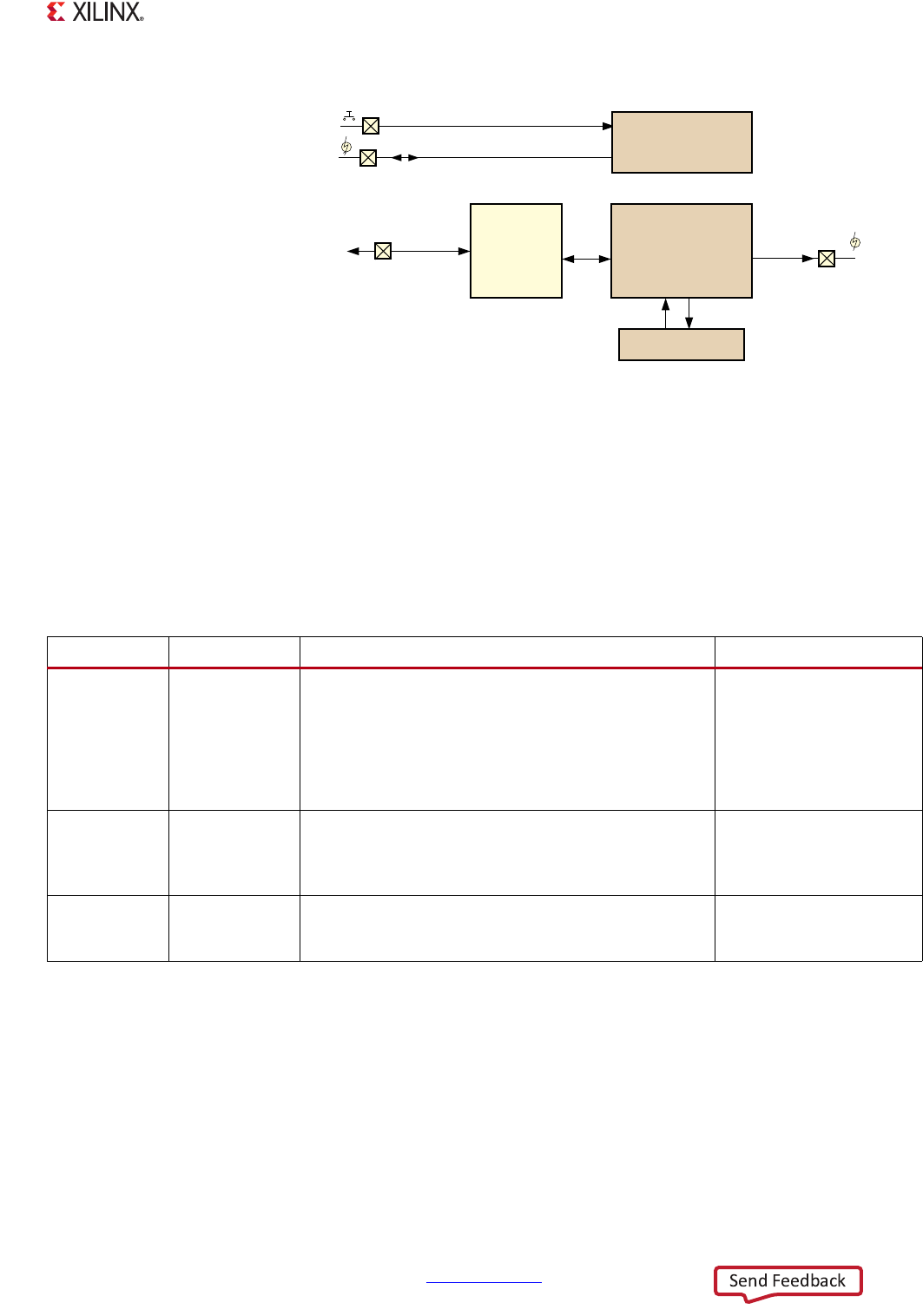
PL User Control and Status Signals
The PROGRAM_B signal can be asserted using a push button to initiate a PL initialization process.
The red LED on the INIT_B signal will turn on when the PL is being initialized and then go out. At this
time, the user can use the TAP controller to configure the PL. There is green LED to indicate when the
DONE signal goes High. This signals that the PL has been successfully programmed. The PL
initialization signal pins are part of the PL voltage domain.
X-Ref Target - Figure 6-20
Figure 6-20: PL Initialization and Configuration Using User-JTAG
-7$*7$3&RQWUROOHU
8*BFBDB
352*5$0B%
3/,QLWLDOL]DWLRQ
&LUFXLWV
3/&RQILJXUDWLRQ
0RGXOH
%LWVWUHDP
-7$*'HEXJ
$(6+0$&8QLWV
>3&$3B35@ [
>3&$3B02'(@
'21(
2'
,1,7B%
&RQILJXUH3/
,QLWLDOL]H3/
Table 6-24: PL Initialization Signals
Signal Name Type Description Board Connection
PROGRAM_B
Active-Low
input
Reset PL Configuration Logic. The PROGRAM_B input
is usually pulsed Low by external means to reset the PL
and allow the PS software or JTAG TAP controller to
program the PL with a bitstream. When PROGRAM_B is
driven Low, the PL initialization sequence begins,
causing the PL to drive the INIT_B signal Low during the
process.
External 4.7 kΩ (or
stronger) pull-up resistor
to V
CCO_0
. Use a push
button to GND to
generate a configuration
reset.
INIT_B
Active-Low
open-drain I/O
PL Initialization Activity and Configuration Error.
The PL drives the INIT_B pin Low when the PL is
initializing (clearing) its configuration memory, or
when the PL has detected a configuration error.
(1)
External 4.7 kΩ (or
stronger) pull-up resistor
to V
CCO_0
to ensure clean
Low-to-High transitions.
DONE
Active-High
open-drain
output
PL Configuration Done Indicator. The PL drives the
DONE signal Low until the PL is successfully
configured.
External 300Ω pull-up
resistor to V
CCO_0
.
Notes:
1. Unlike FPGAs, the INIT_B should not be externally held Low to delay the PL configuration sequence because this is not
indicated in the devcfg.STATUS [PCFG_INIT] register bit that is visible to PS software.