
User manual


Table Of Contents
- Zynq-7000 All Programmable SoC
- Table of Contents
- Ch. 1: Introduction
- Ch. 2: Signals, Interfaces, and Pins
- Ch. 3: Application Processing Unit
- Ch. 4: System Addresses
- Ch. 5: Interconnect
- Ch. 6: Boot and Configuration
- Ch. 7: Interrupts
- Ch. 8: Timers
- Ch. 9: DMA Controller
- Introduction
- Functional Description
- DMA Transfers on the AXI Interconnect
- AXI Transaction Considerations
- DMA Manager
- Multi-channel Data FIFO (MFIFO)
- Memory-to-Memory Transfers
- PL Peripheral AXI Transactions
- PL Peripheral Request Interface
- PL Peripheral - Length Managed by PL Peripheral
- PL Peripheral - Length Managed by DMAC
- Events and Interrupts
- Aborts
- Security
- IP Configuration Options
- Programming Guide for DMA Controller
- Programming Guide for DMA Engine
- Programming Restrictions
- System Functions
- I/O Interface
- Ch. 10: DDR Memory Controller
- Introduction
- AXI Memory Port Interface (DDRI)
- DDR Core and Transaction Scheduler (DDRC)
- DDRC Arbitration
- Controller PHY (DDRP)
- Initialization and Calibration
- DDR Clock Initialization
- DDR IOB Impedance Calibration
- DDR IOB Configuration
- DDR Controller Register Programming
- DRAM Reset and Initialization
- DRAM Input Impedance (ODT) Calibration
- DRAM Output Impedance (RON) Calibration
- DRAM Training
- Write Data Eye Adjustment
- Alternatives to Automatic DRAM Training
- DRAM Write Latency Restriction
- Register Overview
- Error Correction Code (ECC)
- Programming Model
- Ch. 11: Static Memory Controller
- Ch. 12: Quad-SPI Flash Controller
- Ch. 13: SD/SDIO Controller
- Ch. 14: General Purpose I/O (GPIO)
- Ch. 15: USB Host, Device, and OTG Controller
- Introduction
- Functional Description
- Programming Overview and Reference
- Device Mode Control
- Device Endpoint Data Structures
- Device Endpoint Packet Operational Model
- Device Endpoint Descriptor Reference
- Programming Guide for Device Controller
- Programming Guide for Device Endpoint Data Structures
- Host Mode Data Structures
- EHCI Implementation
- Host Data Structures Reference
- Programming Guide for Host Controller
- OTG Description and Reference
- System Functions
- I/O Interfaces
- Ch. 16: Gigabit Ethernet Controller
- Ch. 17: SPI Controller
- Ch. 18: CAN Controller
- Ch. 19: UART Controller
- Ch. 20: I2C Controller
- Ch. 21: Programmable Logic Description
- Ch. 22: Programmable Logic Design Guide
- Ch. 23: Programmable Logic Test and Debug
- Ch. 24: Power Management
- Ch. 25: Clocks
- Ch. 26: Reset System
- Ch. 27: JTAG and DAP Subsystem
- Ch. 28: System Test and Debug
- Ch. 29: On-Chip Memory (OCM)
- Ch. 30: XADC Interface
- Ch. 31: PCI Express
- Ch. 32: Device Secure Boot
- Appx. A: Additional Resources
- Appx. B: Register Details
- Overview
- Acronyms
- Module Summary
- AXI_HP Interface (AFI) (axi_hp)
- CAN Controller (can)
- DDR Memory Controller (ddrc)
- CoreSight Cross Trigger Interface (cti)
- Performance Monitor Unit (cortexa9_pmu)
- CoreSight Program Trace Macrocell (ptm)
- Debug Access Port (dap)
- CoreSight Embedded Trace Buffer (etb)
- PL Fabric Trace Monitor (ftm)
- CoreSight Trace Funnel (funnel)
- CoreSight Intstrumentation Trace Macrocell (itm)
- CoreSight Trace Packet Output (tpiu)
- Device Configuration Interface (devcfg)
- DMA Controller (dmac)
- Gigabit Ethernet Controller (GEM)
- General Purpose I/O (gpio)
- Interconnect QoS (qos301)
- NIC301 Address Region Control (nic301_addr_region_ctrl_registers)
- I2C Controller (IIC)
- L2 Cache (L2Cpl310)
- Application Processing Unit (mpcore)
- On-Chip Memory (ocm)
- Quad-SPI Flash Controller (qspi)
- SD Controller (sdio)
- System Level Control Registers (slcr)
- Static Memory Controller (pl353)
- SPI Controller (SPI)
- System Watchdog Timer (swdt)
- Triple Timer Counter (ttc)
- UART Controller (UART)
- USB Controller (usb)
Zynq-7000 AP SoC Technical Reference Manual www.xilinx.com 221
UG585 (v1.11) September 27, 2016
Chapter 6: Boot and Configuration
• The Zynq-7000 device version (affects the PL initialization time and bitstream load time).
• The size of the loaded images (e.g., Linux image size).
IMPORTANT: The time it takes for each boot and configuration process to complete can be hard to
calculate because of all the variables involved. The values provided here are meant as a guide, not a
definitive answer. If you have any questions, please contact your Xilinx FAE Sales Engineer.
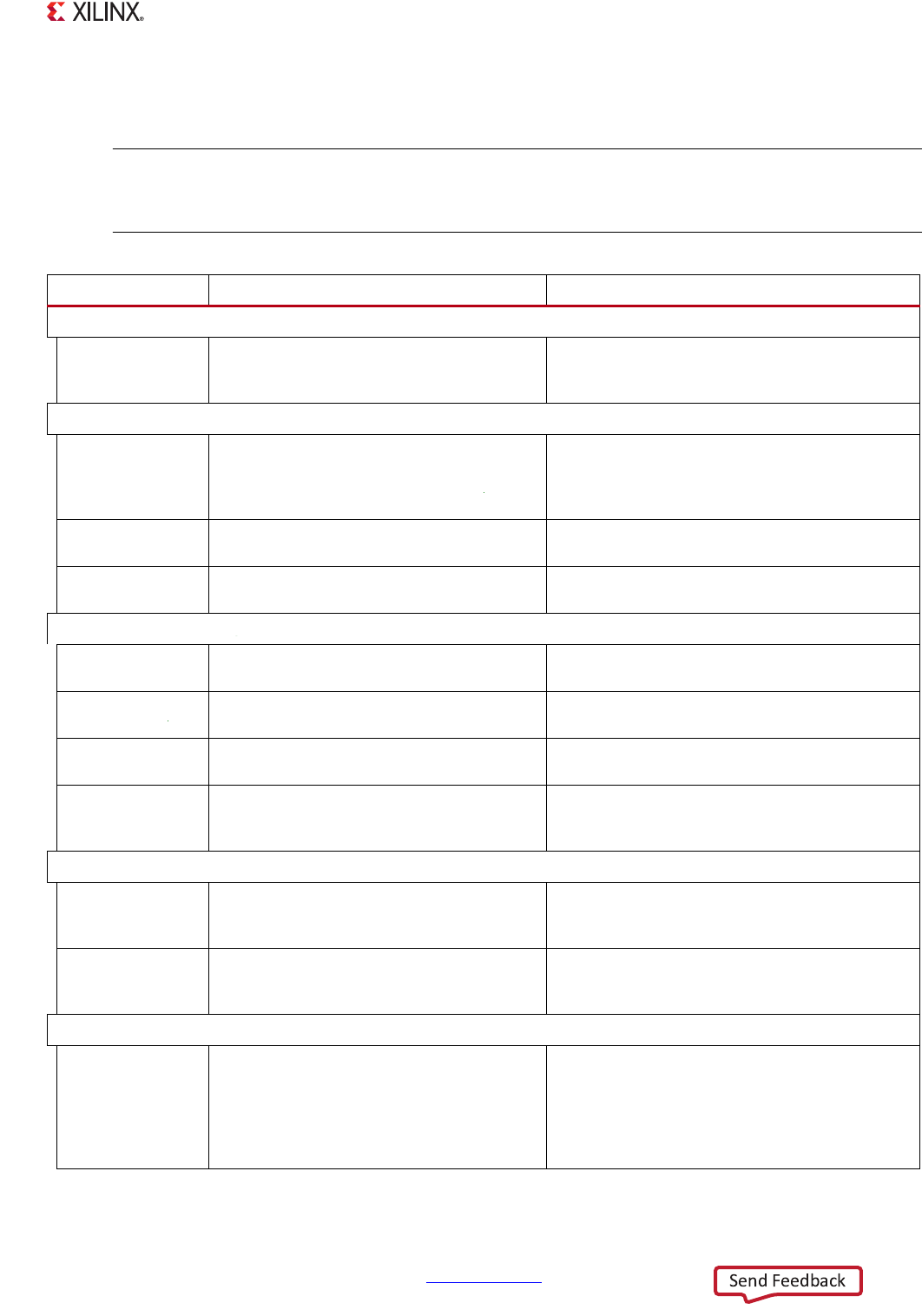
Table 6-25: Factors that Affect Boot and Configuration Time
Functional Area Description Boot Time Considerations
Zynq Device
Version
All device versions share the same PS and
boot time characteristics except when the PL
is involved.
PL size impacts the time for initialization
(cleaning/clearing) and configuration (bitstream).
Security
Encryption
Decryption is required for secure boot.
Software uses the AES unit in the PL.
The decryption time is highly dependent on the
size of the boot image/bitstream and the PS_CLK
frequency. The decryption time is also impacted
by low bandwidth boot devices
(5)
.
HMAC
Authentication
Authentication is done in the HMAC unit in
the PL.
The HMAC authentication time depends on the
PS_CLK frequency and size of the image.
RSA
Authentication
Performed by the BootROM.
The RSA authentication time depends on many
factors
(6)
.
Flash Device Attributes
Boot Device
Vendor and Model
The Flash memory manufacturer and model
impacts performance.
Situations vary
(1)
.
Boot Interface
The performance of the boot device
interface is the most important factor.
Table 6-8 shows relative performances of various
boot devices in a example context.
Boot Interface
Optimization
BootROM Header register initialization is
available.
Improves the read bandwidth of the flash device
all flash accesses
(2)
.
Execute-in-place Quad-SPI and NOR option.
In non-secure mode, allows the CPU to execute
the FSBL/User code without needing to copy it to
the OCM memory.
PS Hardware Requirements
PS Voltage Ramp
This is power supply performance
specification. A fast power supply might
have a 5 to 10 ms voltage ramp time.
The minimum ramp time is provided in the data
sheet.
PS Hardware Boot
After a POR reset, the hardware samples the
strapping pins, does some hardware
housekeeping.
Less than 10 microseconds.
PS Hardware and BootROM Options
PS PLL Startup and
Lock
After a POR, the PLL programming is done
by the hardware before the BootROM
executes. After a non-POR reset the
BootROM re-programs the PLLs and waits
for them to lock before continuing
execution.
PLL lock time is a data sheet specification. Refer
to DS187 or DS191. The three PLLs are enabled by
the BOOT_MODE [4] pin.