
User manual


Table Of Contents
- Zynq-7000 All Programmable SoC
- Table of Contents
- Ch. 1: Introduction
- Ch. 2: Signals, Interfaces, and Pins
- Ch. 3: Application Processing Unit
- Ch. 4: System Addresses
- Ch. 5: Interconnect
- Ch. 6: Boot and Configuration
- Ch. 7: Interrupts
- Ch. 8: Timers
- Ch. 9: DMA Controller
- Introduction
- Functional Description
- DMA Transfers on the AXI Interconnect
- AXI Transaction Considerations
- DMA Manager
- Multi-channel Data FIFO (MFIFO)
- Memory-to-Memory Transfers
- PL Peripheral AXI Transactions
- PL Peripheral Request Interface
- PL Peripheral - Length Managed by PL Peripheral
- PL Peripheral - Length Managed by DMAC
- Events and Interrupts
- Aborts
- Security
- IP Configuration Options
- Programming Guide for DMA Controller
- Programming Guide for DMA Engine
- Programming Restrictions
- System Functions
- I/O Interface
- Ch. 10: DDR Memory Controller
- Introduction
- AXI Memory Port Interface (DDRI)
- DDR Core and Transaction Scheduler (DDRC)
- DDRC Arbitration
- Controller PHY (DDRP)
- Initialization and Calibration
- DDR Clock Initialization
- DDR IOB Impedance Calibration
- DDR IOB Configuration
- DDR Controller Register Programming
- DRAM Reset and Initialization
- DRAM Input Impedance (ODT) Calibration
- DRAM Output Impedance (RON) Calibration
- DRAM Training
- Write Data Eye Adjustment
- Alternatives to Automatic DRAM Training
- DRAM Write Latency Restriction
- Register Overview
- Error Correction Code (ECC)
- Programming Model
- Ch. 11: Static Memory Controller
- Ch. 12: Quad-SPI Flash Controller
- Ch. 13: SD/SDIO Controller
- Ch. 14: General Purpose I/O (GPIO)
- Ch. 15: USB Host, Device, and OTG Controller
- Introduction
- Functional Description
- Programming Overview and Reference
- Device Mode Control
- Device Endpoint Data Structures
- Device Endpoint Packet Operational Model
- Device Endpoint Descriptor Reference
- Programming Guide for Device Controller
- Programming Guide for Device Endpoint Data Structures
- Host Mode Data Structures
- EHCI Implementation
- Host Data Structures Reference
- Programming Guide for Host Controller
- OTG Description and Reference
- System Functions
- I/O Interfaces
- Ch. 16: Gigabit Ethernet Controller
- Ch. 17: SPI Controller
- Ch. 18: CAN Controller
- Ch. 19: UART Controller
- Ch. 20: I2C Controller
- Ch. 21: Programmable Logic Description
- Ch. 22: Programmable Logic Design Guide
- Ch. 23: Programmable Logic Test and Debug
- Ch. 24: Power Management
- Ch. 25: Clocks
- Ch. 26: Reset System
- Ch. 27: JTAG and DAP Subsystem
- Ch. 28: System Test and Debug
- Ch. 29: On-Chip Memory (OCM)
- Ch. 30: XADC Interface
- Ch. 31: PCI Express
- Ch. 32: Device Secure Boot
- Appx. A: Additional Resources
- Appx. B: Register Details
- Overview
- Acronyms
- Module Summary
- AXI_HP Interface (AFI) (axi_hp)
- CAN Controller (can)
- DDR Memory Controller (ddrc)
- CoreSight Cross Trigger Interface (cti)
- Performance Monitor Unit (cortexa9_pmu)
- CoreSight Program Trace Macrocell (ptm)
- Debug Access Port (dap)
- CoreSight Embedded Trace Buffer (etb)
- PL Fabric Trace Monitor (ftm)
- CoreSight Trace Funnel (funnel)
- CoreSight Intstrumentation Trace Macrocell (itm)
- CoreSight Trace Packet Output (tpiu)
- Device Configuration Interface (devcfg)
- DMA Controller (dmac)
- Gigabit Ethernet Controller (GEM)
- General Purpose I/O (gpio)
- Interconnect QoS (qos301)
- NIC301 Address Region Control (nic301_addr_region_ctrl_registers)
- I2C Controller (IIC)
- L2 Cache (L2Cpl310)
- Application Processing Unit (mpcore)
- On-Chip Memory (ocm)
- Quad-SPI Flash Controller (qspi)
- SD Controller (sdio)
- System Level Control Registers (slcr)
- Static Memory Controller (pl353)
- SPI Controller (SPI)
- System Watchdog Timer (swdt)
- Triple Timer Counter (ttc)
- UART Controller (UART)
- USB Controller (usb)
Zynq-7000 AP SoC Technical Reference Manual www.xilinx.com 228
UG585 (v1.11) September 27, 2016
Chapter 7: Interrupts
All SGIs are edge triggered. The sensitivity types for SGIs are fixed and cannot be changed; the
ICDICFR0 register is read-only, since it specifies the sensitivity types of all the 16 SGIs.
7.2.2 CPU Private Peripheral Interrupts (PPI)
Each CPU connects to a private set of five peripheral interrupts. The PPIs are listed in Table 7-3.
The sensitivity types for PPIs are fixed and cannot be changed; therefore, the ICDICFR1 register is
read-only, since it specifies the sensitivity types of all the 5 PPIs. Note that the fast interrupt (FIQ)
signal and the interrupt (IRQ) signal from the PL are inverted and then sent to the interrupt
controller. Therefore, they are active High at the PS-PL interface, although the ICDICFR1 register
reflects them as active Low level.
7.2.3 Shared Peripheral Interrupts (SPI)
A group of approximately 60 interrupts from various modules can be routed to one or both of the
CPUs or the PL. The interrupt controller manages the prioritization and reception of these interrupts
for the CPUs.
Except for IRQ #61 through #68 and #84 through #91, all interrupt sensitivity types are fixed by the
requesting sources and cannot be changed. The GIC must be programmed to accommodate this. The
boot ROM does not program these registers; therefore the SDK device drivers must program the GIC
to accommodate these sensitivity types.
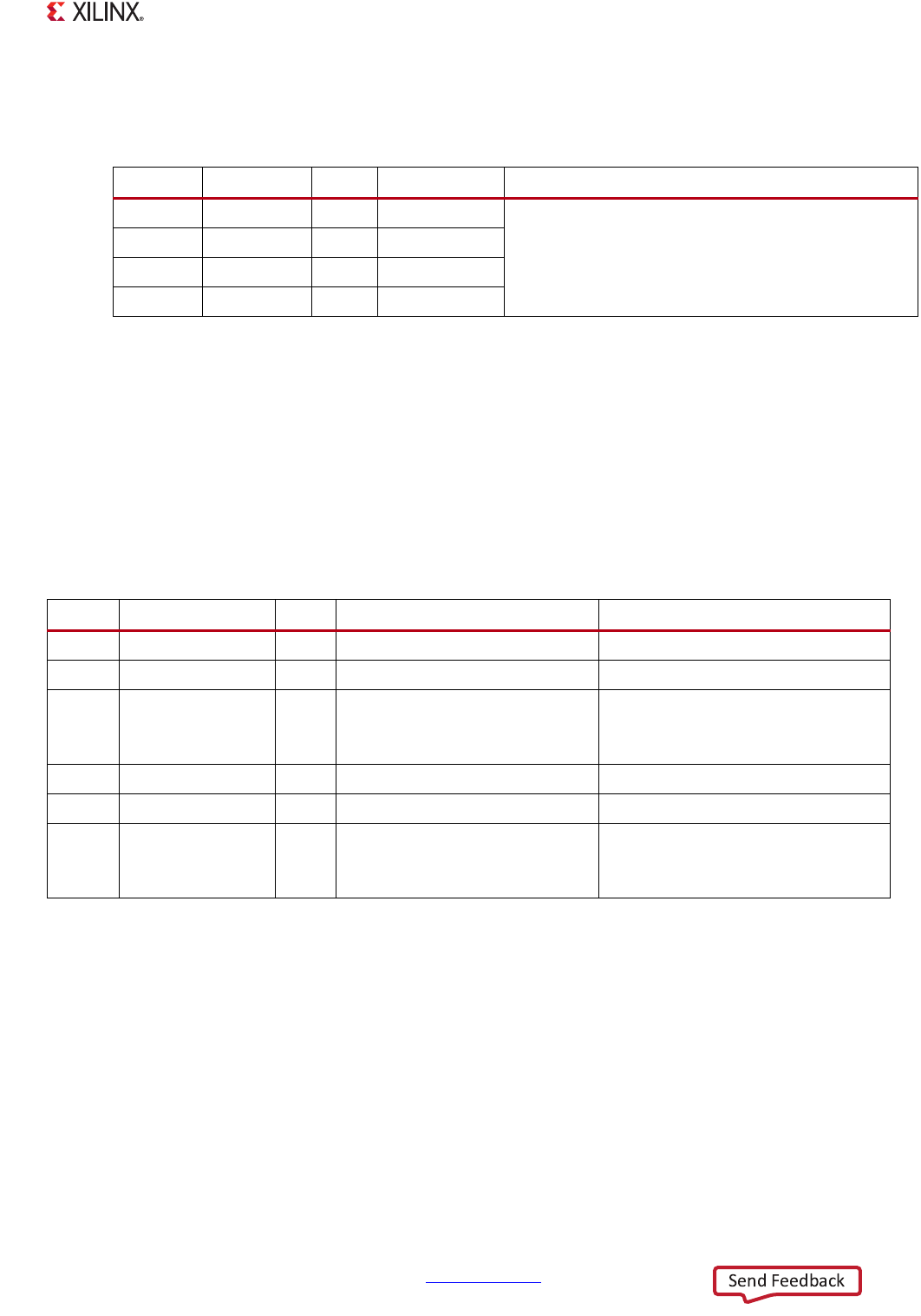
Table 7-2: Software Generated Interrupts (SGI)
IRQ ID# Name SGI# Type Description
0 Software 0 0 Rising edge A set of 16 interrupt sources that are private to each
CPU that can be routed to up to 16 common interrupt
destinations where each destination can be one or
more CPUs.
1 Software 1 1 Rising edge
~ ... ~ ...
15 Software 15 15 Rising edge
Table 7-3: Private Peripheral Interrupts (PPI)
IRQ ID# Name PPI# Type Description
26:16 Reserved ~ ~ Reserved
27 Global Timer 0 Rising edge Global timer
28 nFIQ 1
Active Low level
(active High at PS-PL interface)
Fast interrupt signal from the PL:
CPU0: IRQF2P[18]
CPU1: IRQF2P[19]
29 CPU Private Timer 2 Rising edge Interrupt from private CPU timer
30 AWDT{0, 1} 3 Rising edge Private watchdog timer for each CPU
31 nIRQ 4
Active Low level
(active High at PS-PL interface)
Interrupt signal from the PL:
CPU0: IRQF2P[16]
CPU1: IRQF2P[17]