
User manual


Table Of Contents
- Zynq-7000 All Programmable SoC
- Table of Contents
- Ch. 1: Introduction
- Ch. 2: Signals, Interfaces, and Pins
- Ch. 3: Application Processing Unit
- Ch. 4: System Addresses
- Ch. 5: Interconnect
- Ch. 6: Boot and Configuration
- Ch. 7: Interrupts
- Ch. 8: Timers
- Ch. 9: DMA Controller
- Introduction
- Functional Description
- DMA Transfers on the AXI Interconnect
- AXI Transaction Considerations
- DMA Manager
- Multi-channel Data FIFO (MFIFO)
- Memory-to-Memory Transfers
- PL Peripheral AXI Transactions
- PL Peripheral Request Interface
- PL Peripheral - Length Managed by PL Peripheral
- PL Peripheral - Length Managed by DMAC
- Events and Interrupts
- Aborts
- Security
- IP Configuration Options
- Programming Guide for DMA Controller
- Programming Guide for DMA Engine
- Programming Restrictions
- System Functions
- I/O Interface
- Ch. 10: DDR Memory Controller
- Introduction
- AXI Memory Port Interface (DDRI)
- DDR Core and Transaction Scheduler (DDRC)
- DDRC Arbitration
- Controller PHY (DDRP)
- Initialization and Calibration
- DDR Clock Initialization
- DDR IOB Impedance Calibration
- DDR IOB Configuration
- DDR Controller Register Programming
- DRAM Reset and Initialization
- DRAM Input Impedance (ODT) Calibration
- DRAM Output Impedance (RON) Calibration
- DRAM Training
- Write Data Eye Adjustment
- Alternatives to Automatic DRAM Training
- DRAM Write Latency Restriction
- Register Overview
- Error Correction Code (ECC)
- Programming Model
- Ch. 11: Static Memory Controller
- Ch. 12: Quad-SPI Flash Controller
- Ch. 13: SD/SDIO Controller
- Ch. 14: General Purpose I/O (GPIO)
- Ch. 15: USB Host, Device, and OTG Controller
- Introduction
- Functional Description
- Programming Overview and Reference
- Device Mode Control
- Device Endpoint Data Structures
- Device Endpoint Packet Operational Model
- Device Endpoint Descriptor Reference
- Programming Guide for Device Controller
- Programming Guide for Device Endpoint Data Structures
- Host Mode Data Structures
- EHCI Implementation
- Host Data Structures Reference
- Programming Guide for Host Controller
- OTG Description and Reference
- System Functions
- I/O Interfaces
- Ch. 16: Gigabit Ethernet Controller
- Ch. 17: SPI Controller
- Ch. 18: CAN Controller
- Ch. 19: UART Controller
- Ch. 20: I2C Controller
- Ch. 21: Programmable Logic Description
- Ch. 22: Programmable Logic Design Guide
- Ch. 23: Programmable Logic Test and Debug
- Ch. 24: Power Management
- Ch. 25: Clocks
- Ch. 26: Reset System
- Ch. 27: JTAG and DAP Subsystem
- Ch. 28: System Test and Debug
- Ch. 29: On-Chip Memory (OCM)
- Ch. 30: XADC Interface
- Ch. 31: PCI Express
- Ch. 32: Device Secure Boot
- Appx. A: Additional Resources
- Appx. B: Register Details
- Overview
- Acronyms
- Module Summary
- AXI_HP Interface (AFI) (axi_hp)
- CAN Controller (can)
- DDR Memory Controller (ddrc)
- CoreSight Cross Trigger Interface (cti)
- Performance Monitor Unit (cortexa9_pmu)
- CoreSight Program Trace Macrocell (ptm)
- Debug Access Port (dap)
- CoreSight Embedded Trace Buffer (etb)
- PL Fabric Trace Monitor (ftm)
- CoreSight Trace Funnel (funnel)
- CoreSight Intstrumentation Trace Macrocell (itm)
- CoreSight Trace Packet Output (tpiu)
- Device Configuration Interface (devcfg)
- DMA Controller (dmac)
- Gigabit Ethernet Controller (GEM)
- General Purpose I/O (gpio)
- Interconnect QoS (qos301)
- NIC301 Address Region Control (nic301_addr_region_ctrl_registers)
- I2C Controller (IIC)
- L2 Cache (L2Cpl310)
- Application Processing Unit (mpcore)
- On-Chip Memory (ocm)
- Quad-SPI Flash Controller (qspi)
- SD Controller (sdio)
- System Level Control Registers (slcr)
- Static Memory Controller (pl353)
- SPI Controller (SPI)
- System Watchdog Timer (swdt)
- Triple Timer Counter (ttc)
- UART Controller (UART)
- USB Controller (usb)
Zynq-7000 AP SoC Technical Reference Manual www.xilinx.com 231
UG585 (v1.11) September 27, 2016
Chapter 7: Interrupts
Table 7-4, PS and PL Shared Peripheral Interrupts (SPI). The sensitivity is programmed using the
ICDICFR [5:2] registers.
Private Peripheral Interrupts (PPI)
Each CPU has its own separate PPI interrupts with fixed functionality; the sensitivity, handling, and
targeting of these interrupts are not programmable. Each interrupt only goes to its own CPU and is
handled by that CPU. The ICDICFR [1] register is read-only and the ICDIPTR [5:2] registers are
essentially reserved.
Software Generated Interrupts (SGI)
The SGI interrupts are always edge sensitive and are generated when software writes the interrupt
number to ICDSGIR register. All of the targeted CPUs defined in the ICDIPTR [23:8] must handle the
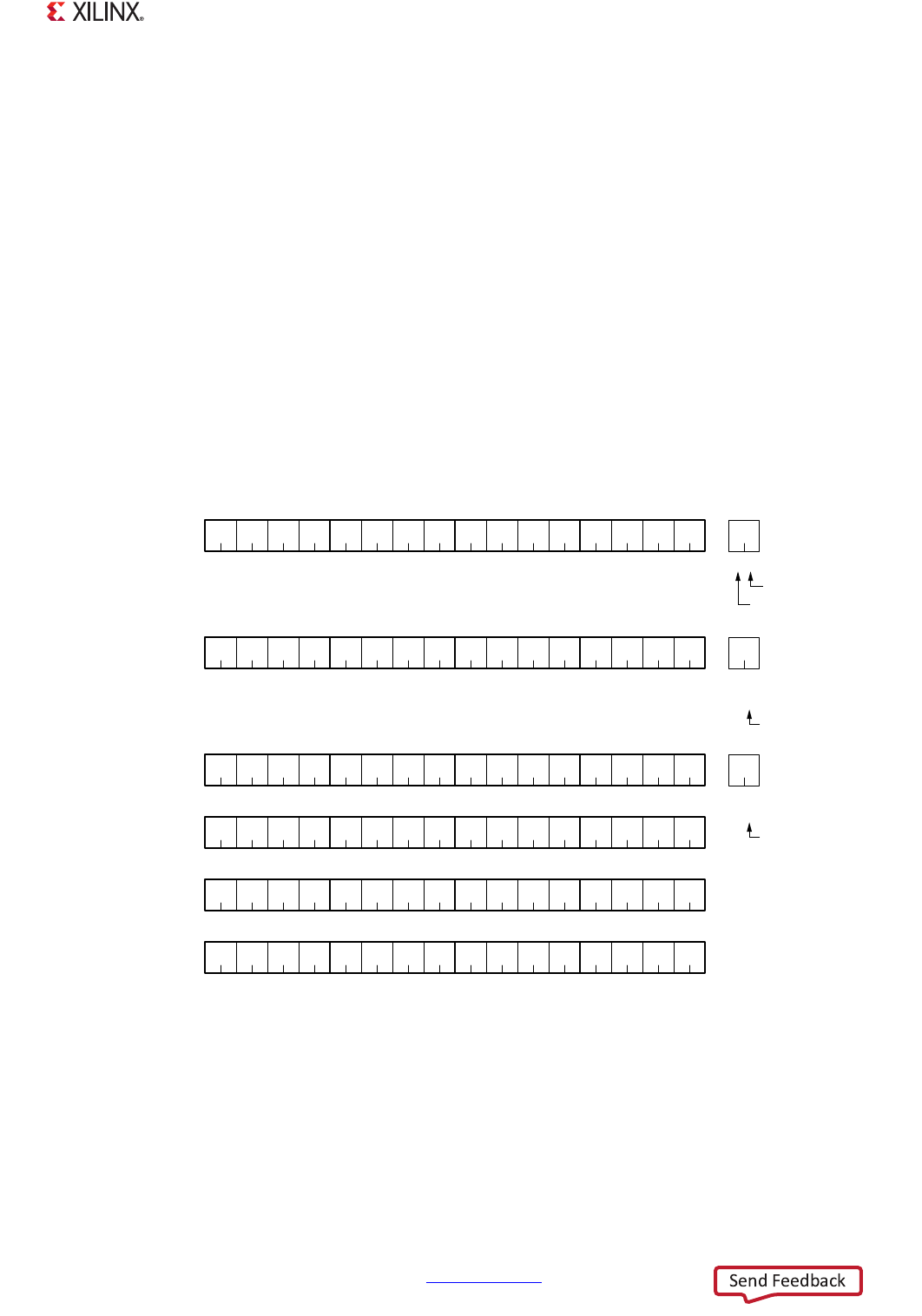
interrupt in order to clear it. See Figure 7-4 and Figure 7-5.
X-Ref Target - Figure 7-4
Figure 7-4: Interrupts ICDICFR Register for Sensitivity and Handling
Private Peripheral Interrupts (PPI)
62
63 61 60
Shared Peripheral Interrupts (SPI)
58
59 57 56 5455 53 52 5051 49 48
ICD ICFR 3
78
79 77 76 7475 73 72 7071 69 68 6667 65 64
ICD ICFR 4
x
31
xx92 9091 89 88 8687 85 84 8283 81 80
24 16 8 0
ICD ICFR 5
46
47 45 44 4243 41 40 3839 37 x 3435 33 32
ICD ICFR 2
30
31 29 28
Software Generated Interrupts (SGI)
x
27 x x xxxx xxxx
ICD ICFR 1
14
15 13 12 1011 9 8 6754 2310
ICD ICFR 0
Edge sensitive.
01: High-level active.
11: Rising-edge active.
IRQ
IRQ
Read-only.
0xAAAA AAAA
Read-only.
0x7DC0 0000
01: Low-level active.
11 : Edge sensitive.
IRQ
(IRQ ID #36, 93, 94 and 95 are reserved.)
Private CPU only.
Other bit combinations
are reserved.
1 0
All targeted CPUs must
handle the interrupt
.
Handled by one CPU.
Sensitivity and
CPU handling model:
UG585_c7_04_121613