
User manual


Table Of Contents
- Zynq-7000 All Programmable SoC
- Table of Contents
- Ch. 1: Introduction
- Ch. 2: Signals, Interfaces, and Pins
- Ch. 3: Application Processing Unit
- Ch. 4: System Addresses
- Ch. 5: Interconnect
- Ch. 6: Boot and Configuration
- Ch. 7: Interrupts
- Ch. 8: Timers
- Ch. 9: DMA Controller
- Introduction
- Functional Description
- DMA Transfers on the AXI Interconnect
- AXI Transaction Considerations
- DMA Manager
- Multi-channel Data FIFO (MFIFO)
- Memory-to-Memory Transfers
- PL Peripheral AXI Transactions
- PL Peripheral Request Interface
- PL Peripheral - Length Managed by PL Peripheral
- PL Peripheral - Length Managed by DMAC
- Events and Interrupts
- Aborts
- Security
- IP Configuration Options
- Programming Guide for DMA Controller
- Programming Guide for DMA Engine
- Programming Restrictions
- System Functions
- I/O Interface
- Ch. 10: DDR Memory Controller
- Introduction
- AXI Memory Port Interface (DDRI)
- DDR Core and Transaction Scheduler (DDRC)
- DDRC Arbitration
- Controller PHY (DDRP)
- Initialization and Calibration
- DDR Clock Initialization
- DDR IOB Impedance Calibration
- DDR IOB Configuration
- DDR Controller Register Programming
- DRAM Reset and Initialization
- DRAM Input Impedance (ODT) Calibration
- DRAM Output Impedance (RON) Calibration
- DRAM Training
- Write Data Eye Adjustment
- Alternatives to Automatic DRAM Training
- DRAM Write Latency Restriction
- Register Overview
- Error Correction Code (ECC)
- Programming Model
- Ch. 11: Static Memory Controller
- Ch. 12: Quad-SPI Flash Controller
- Ch. 13: SD/SDIO Controller
- Ch. 14: General Purpose I/O (GPIO)
- Ch. 15: USB Host, Device, and OTG Controller
- Introduction
- Functional Description
- Programming Overview and Reference
- Device Mode Control
- Device Endpoint Data Structures
- Device Endpoint Packet Operational Model
- Device Endpoint Descriptor Reference
- Programming Guide for Device Controller
- Programming Guide for Device Endpoint Data Structures
- Host Mode Data Structures
- EHCI Implementation
- Host Data Structures Reference
- Programming Guide for Host Controller
- OTG Description and Reference
- System Functions
- I/O Interfaces
- Ch. 16: Gigabit Ethernet Controller
- Ch. 17: SPI Controller
- Ch. 18: CAN Controller
- Ch. 19: UART Controller
- Ch. 20: I2C Controller
- Ch. 21: Programmable Logic Description
- Ch. 22: Programmable Logic Design Guide
- Ch. 23: Programmable Logic Test and Debug
- Ch. 24: Power Management
- Ch. 25: Clocks
- Ch. 26: Reset System
- Ch. 27: JTAG and DAP Subsystem
- Ch. 28: System Test and Debug
- Ch. 29: On-Chip Memory (OCM)
- Ch. 30: XADC Interface
- Ch. 31: PCI Express
- Ch. 32: Device Secure Boot
- Appx. A: Additional Resources
- Appx. B: Register Details
- Overview
- Acronyms
- Module Summary
- AXI_HP Interface (AFI) (axi_hp)
- CAN Controller (can)
- DDR Memory Controller (ddrc)
- CoreSight Cross Trigger Interface (cti)
- Performance Monitor Unit (cortexa9_pmu)
- CoreSight Program Trace Macrocell (ptm)
- Debug Access Port (dap)
- CoreSight Embedded Trace Buffer (etb)
- PL Fabric Trace Monitor (ftm)
- CoreSight Trace Funnel (funnel)
- CoreSight Intstrumentation Trace Macrocell (itm)
- CoreSight Trace Packet Output (tpiu)
- Device Configuration Interface (devcfg)
- DMA Controller (dmac)
- Gigabit Ethernet Controller (GEM)
- General Purpose I/O (gpio)
- Interconnect QoS (qos301)
- NIC301 Address Region Control (nic301_addr_region_ctrl_registers)
- I2C Controller (IIC)
- L2 Cache (L2Cpl310)
- Application Processing Unit (mpcore)
- On-Chip Memory (ocm)
- Quad-SPI Flash Controller (qspi)
- SD Controller (sdio)
- System Level Control Registers (slcr)
- Static Memory Controller (pl353)
- SPI Controller (SPI)
- System Watchdog Timer (swdt)
- Triple Timer Counter (ttc)
- UART Controller (UART)
- USB Controller (usb)
Zynq-7000 AP SoC Technical Reference Manual www.xilinx.com 232
UG585 (v1.11) September 27, 2016
Chapter 7: Interrupts
7.2.5 Wait for Interrupt Event Signal (WFI)
The CPU can go into a wait state where it waits for an interrupt (or event) signal to be generated. The
wait for interrupt signal that is sent to the PL is described in Chapter 3, Application Processing Unit.
7.3 Register Overview
The ICC and ICD registers are part of the pl390 GIC register set. There are 60 SPI interrupts. This is far
fewer than what the pl390 can support, so there are far fewer interrupt enable, status, prioritization
and processor target registers in the ICD than is possible for the pl390. A summary of the ICC and ICD
registers are listed in Table 7-5
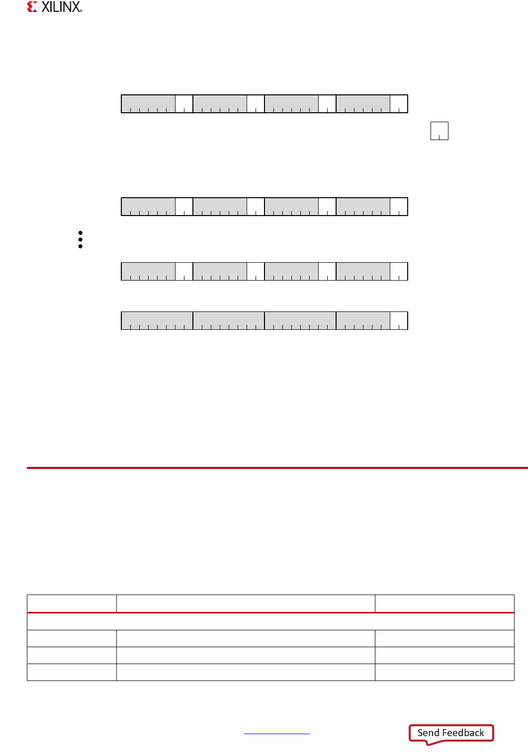
X-Ref Target - Figure 7-5
Figure 7-5: Interrupts ICDIPTR Register for Targeting CPU
reserved
31 24 16 8 0
IRQ # 3
ICD IPTR [3:0]
00: not targeted
01: targeted to CPU 0
10: targeted to CPU 1
11: targeted to both CPUs
reserved reserved reserved
IRQ # 2 IRQ # 1 IRQ # 0
31 24 16 8 0
ICD IPTR [8]
reserved
IRQ # 35
reserved reserved reserved
IRQ # 34 IRQ # 33 IRQ # 32
ICD IPTR [22]
reserved
IRQ # 91
reserved reserved reserved
IRQ # 90 IRQ # 89 IRQ # 88
ICD IPTR [23]
IRQ # 95
reserved
IRQ # 94 IRQ # 93 IRQ # 92
reserved reserved reserved
IRQ # 7 IRQ # 6 IRQ # 5 IRQ # 4
IRQ # 11 IRQ # 10 IRQ # 9 IRQ # 8
IRQ # 15 IRQ # 14 IRQ # 13 IRQ # 12
ICD IPTR [7:4]
Reserved, these interrupts are always targeted to their private CPU.
IRQ # 36, 93, 94, and
95 are reserved.
SGI
PPI
SPI
SPI
SPI
UG585_c7_05_121613
Table 7-5: Interrupt Controller Register Overview
Name
Register Description Write Protection Lock
Interrupt Controller CPU (ICC)
ICCICR CPU interface control Yes, except EnableNS
ICCPMR Interrupt priority mask ~
ICCBPR Binary point for interrupt priority ~