
User manual


Table Of Contents
- Zynq-7000 All Programmable SoC
- Table of Contents
- Ch. 1: Introduction
- Ch. 2: Signals, Interfaces, and Pins
- Ch. 3: Application Processing Unit
- Ch. 4: System Addresses
- Ch. 5: Interconnect
- Ch. 6: Boot and Configuration
- Ch. 7: Interrupts
- Ch. 8: Timers
- Ch. 9: DMA Controller
- Introduction
- Functional Description
- DMA Transfers on the AXI Interconnect
- AXI Transaction Considerations
- DMA Manager
- Multi-channel Data FIFO (MFIFO)
- Memory-to-Memory Transfers
- PL Peripheral AXI Transactions
- PL Peripheral Request Interface
- PL Peripheral - Length Managed by PL Peripheral
- PL Peripheral - Length Managed by DMAC
- Events and Interrupts
- Aborts
- Security
- IP Configuration Options
- Programming Guide for DMA Controller
- Programming Guide for DMA Engine
- Programming Restrictions
- System Functions
- I/O Interface
- Ch. 10: DDR Memory Controller
- Introduction
- AXI Memory Port Interface (DDRI)
- DDR Core and Transaction Scheduler (DDRC)
- DDRC Arbitration
- Controller PHY (DDRP)
- Initialization and Calibration
- DDR Clock Initialization
- DDR IOB Impedance Calibration
- DDR IOB Configuration
- DDR Controller Register Programming
- DRAM Reset and Initialization
- DRAM Input Impedance (ODT) Calibration
- DRAM Output Impedance (RON) Calibration
- DRAM Training
- Write Data Eye Adjustment
- Alternatives to Automatic DRAM Training
- DRAM Write Latency Restriction
- Register Overview
- Error Correction Code (ECC)
- Programming Model
- Ch. 11: Static Memory Controller
- Ch. 12: Quad-SPI Flash Controller
- Ch. 13: SD/SDIO Controller
- Ch. 14: General Purpose I/O (GPIO)
- Ch. 15: USB Host, Device, and OTG Controller
- Introduction
- Functional Description
- Programming Overview and Reference
- Device Mode Control
- Device Endpoint Data Structures
- Device Endpoint Packet Operational Model
- Device Endpoint Descriptor Reference
- Programming Guide for Device Controller
- Programming Guide for Device Endpoint Data Structures
- Host Mode Data Structures
- EHCI Implementation
- Host Data Structures Reference
- Programming Guide for Host Controller
- OTG Description and Reference
- System Functions
- I/O Interfaces
- Ch. 16: Gigabit Ethernet Controller
- Ch. 17: SPI Controller
- Ch. 18: CAN Controller
- Ch. 19: UART Controller
- Ch. 20: I2C Controller
- Ch. 21: Programmable Logic Description
- Ch. 22: Programmable Logic Design Guide
- Ch. 23: Programmable Logic Test and Debug
- Ch. 24: Power Management
- Ch. 25: Clocks
- Ch. 26: Reset System
- Ch. 27: JTAG and DAP Subsystem
- Ch. 28: System Test and Debug
- Ch. 29: On-Chip Memory (OCM)
- Ch. 30: XADC Interface
- Ch. 31: PCI Express
- Ch. 32: Device Secure Boot
- Appx. A: Additional Resources
- Appx. B: Register Details
- Overview
- Acronyms
- Module Summary
- AXI_HP Interface (AFI) (axi_hp)
- CAN Controller (can)
- DDR Memory Controller (ddrc)
- CoreSight Cross Trigger Interface (cti)
- Performance Monitor Unit (cortexa9_pmu)
- CoreSight Program Trace Macrocell (ptm)
- Debug Access Port (dap)
- CoreSight Embedded Trace Buffer (etb)
- PL Fabric Trace Monitor (ftm)
- CoreSight Trace Funnel (funnel)
- CoreSight Intstrumentation Trace Macrocell (itm)
- CoreSight Trace Packet Output (tpiu)
- Device Configuration Interface (devcfg)
- DMA Controller (dmac)
- Gigabit Ethernet Controller (GEM)
- General Purpose I/O (gpio)
- Interconnect QoS (qos301)
- NIC301 Address Region Control (nic301_addr_region_ctrl_registers)
- I2C Controller (IIC)
- L2 Cache (L2Cpl310)
- Application Processing Unit (mpcore)
- On-Chip Memory (ocm)
- Quad-SPI Flash Controller (qspi)
- SD Controller (sdio)
- System Level Control Registers (slcr)
- Static Memory Controller (pl353)
- SPI Controller (SPI)
- System Watchdog Timer (swdt)
- Triple Timer Counter (ttc)
- UART Controller (UART)
- USB Controller (usb)
Zynq-7000 AP SoC Technical Reference Manual www.xilinx.com 233
UG585 (v1.11) September 27, 2016
Chapter 7: Interrupts
7.3.1 Write Protection Lock
The interrupt controller provides the facility to prevent write accesses to critical configuration
registers. This is done by writing a one to the APU_CTRL[CFGSDISABLE] bit. The APU_CTRL register is
part of the AP SoC’s System Level Control register set, SLCR. This controls the write behavior for the
secure interrupt control registers.
RECOMMENDED: If the user wants to set the CFGSDISABLE bit, it is recommended that this be done
during the user software boot process which occurs after the software has configured the Interrupt
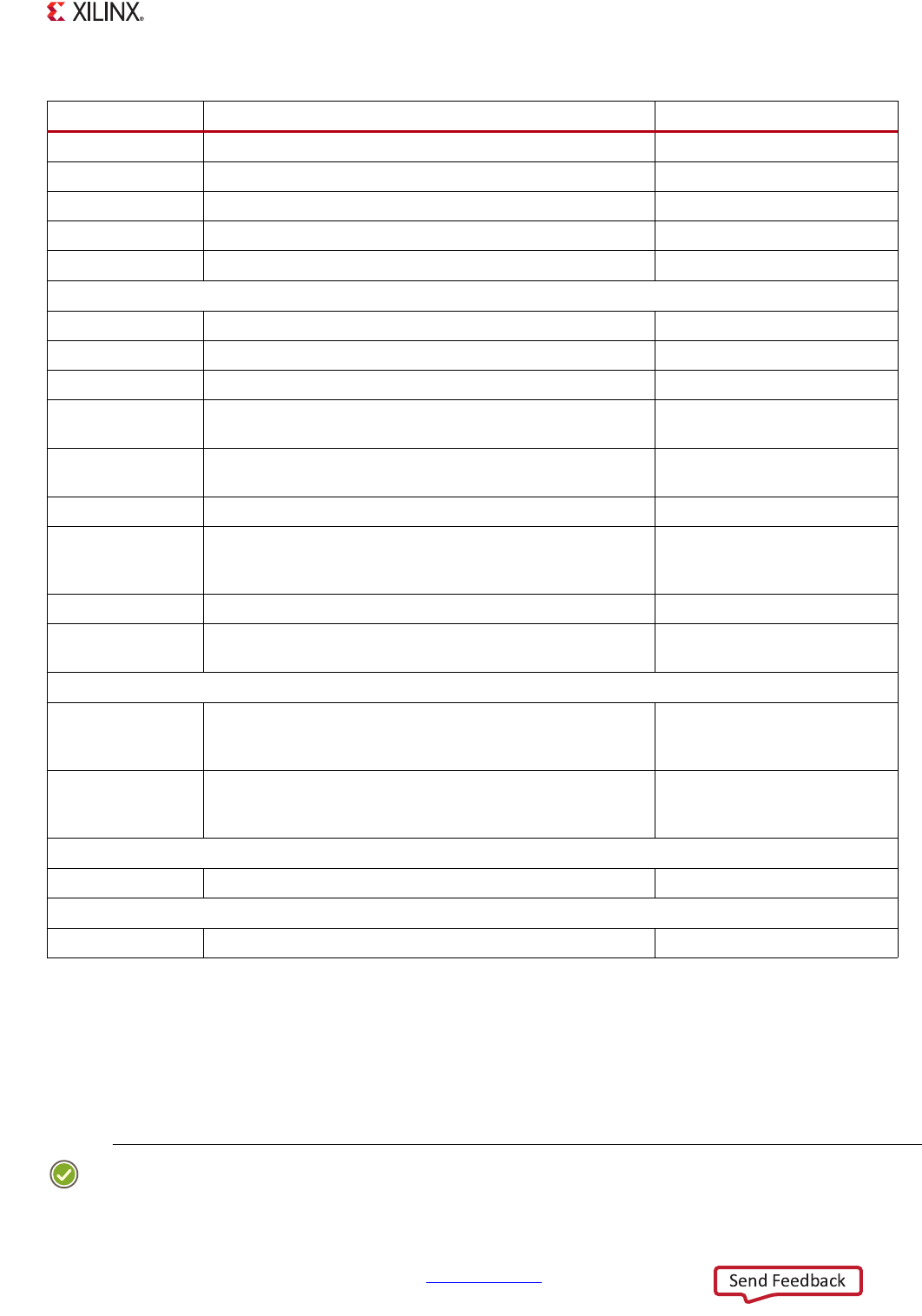
ICCIAR Interrupt acknowledge ~
ICCEOIR End of interrupt ~
ICCRPR Running priority ~
ICCHPIR Highest pending interrupt ~
ICCABPR
Aliased non-secure binary point
~
Interrupt Controller Distributor (ICD)
ICDDCR Secure/non-secure mode select Yes
ICDICTR, ICDIIDR Controller implementation ~
ICDISR [2:0] Interrupt security Yes
ICDISER [2:0],
ICDICER [2:0]
Interrupt set-enable and clear-enable
Yes
ICDISPR [2:0],
ICDICPR [2:0]
Interrupt set-pending and clear-pending
Yes
ICDABR [2:0] Interrupt active ~
ICDIPR [23:0] Interrupt priority, 8-bit fields. Only the upper 7 bits of each
8-bit field are writable; the lowest bit is always 0. This means
the AP SoC supports 128 priority levels, all even values.
Yes
ICDIPTR [23:0] Interrupt processor targets, 8-bit fields. Yes
ICDICFR [5:0] Interrupt sensitivity type, 2-bit fields (level/edge, handling
model)
Yes
PPI and SPI Status
PPI_STATUS PPI status: Corresponds to ICDISR[0], ICDISER[0], ICDICER[0],
ICDISPR[0], ICDICPR[0], and ICDABR[0] registers (security,
enable, pending and active).
~
SPI_STATUS [2:1] SPI status: Corresponds to ICDISR[2:1], ICDISER[2:1],
ICDICER[2:1], ICDISPR[2:1], ICDICPR[2:1], and ICDABR[2:1]
registers (security, enable, pending and active).
~
Software Generated Interrupts (SGI)
ICDSGIR Software-generated interrupts ~
Disable Write Accesses (SLCR register)
APU_CTRL CFGSDISABLE bit disables some write accesses ~
Table 7-5: Interrupt Controller Register Overview (Cont’d)
Name
Register Description Write Protection Lock