
User manual


Table Of Contents
- Zynq-7000 All Programmable SoC
- Table of Contents
- Ch. 1: Introduction
- Ch. 2: Signals, Interfaces, and Pins
- Ch. 3: Application Processing Unit
- Ch. 4: System Addresses
- Ch. 5: Interconnect
- Ch. 6: Boot and Configuration
- Ch. 7: Interrupts
- Ch. 8: Timers
- Ch. 9: DMA Controller
- Introduction
- Functional Description
- DMA Transfers on the AXI Interconnect
- AXI Transaction Considerations
- DMA Manager
- Multi-channel Data FIFO (MFIFO)
- Memory-to-Memory Transfers
- PL Peripheral AXI Transactions
- PL Peripheral Request Interface
- PL Peripheral - Length Managed by PL Peripheral
- PL Peripheral - Length Managed by DMAC
- Events and Interrupts
- Aborts
- Security
- IP Configuration Options
- Programming Guide for DMA Controller
- Programming Guide for DMA Engine
- Programming Restrictions
- System Functions
- I/O Interface
- Ch. 10: DDR Memory Controller
- Introduction
- AXI Memory Port Interface (DDRI)
- DDR Core and Transaction Scheduler (DDRC)
- DDRC Arbitration
- Controller PHY (DDRP)
- Initialization and Calibration
- DDR Clock Initialization
- DDR IOB Impedance Calibration
- DDR IOB Configuration
- DDR Controller Register Programming
- DRAM Reset and Initialization
- DRAM Input Impedance (ODT) Calibration
- DRAM Output Impedance (RON) Calibration
- DRAM Training
- Write Data Eye Adjustment
- Alternatives to Automatic DRAM Training
- DRAM Write Latency Restriction
- Register Overview
- Error Correction Code (ECC)
- Programming Model
- Ch. 11: Static Memory Controller
- Ch. 12: Quad-SPI Flash Controller
- Ch. 13: SD/SDIO Controller
- Ch. 14: General Purpose I/O (GPIO)
- Ch. 15: USB Host, Device, and OTG Controller
- Introduction
- Functional Description
- Programming Overview and Reference
- Device Mode Control
- Device Endpoint Data Structures
- Device Endpoint Packet Operational Model
- Device Endpoint Descriptor Reference
- Programming Guide for Device Controller
- Programming Guide for Device Endpoint Data Structures
- Host Mode Data Structures
- EHCI Implementation
- Host Data Structures Reference
- Programming Guide for Host Controller
- OTG Description and Reference
- System Functions
- I/O Interfaces
- Ch. 16: Gigabit Ethernet Controller
- Ch. 17: SPI Controller
- Ch. 18: CAN Controller
- Ch. 19: UART Controller
- Ch. 20: I2C Controller
- Ch. 21: Programmable Logic Description
- Ch. 22: Programmable Logic Design Guide
- Ch. 23: Programmable Logic Test and Debug
- Ch. 24: Power Management
- Ch. 25: Clocks
- Ch. 26: Reset System
- Ch. 27: JTAG and DAP Subsystem
- Ch. 28: System Test and Debug
- Ch. 29: On-Chip Memory (OCM)
- Ch. 30: XADC Interface
- Ch. 31: PCI Express
- Ch. 32: Device Secure Boot
- Appx. A: Additional Resources
- Appx. B: Register Details
- Overview
- Acronyms
- Module Summary
- AXI_HP Interface (AFI) (axi_hp)
- CAN Controller (can)
- DDR Memory Controller (ddrc)
- CoreSight Cross Trigger Interface (cti)
- Performance Monitor Unit (cortexa9_pmu)
- CoreSight Program Trace Macrocell (ptm)
- Debug Access Port (dap)
- CoreSight Embedded Trace Buffer (etb)
- PL Fabric Trace Monitor (ftm)
- CoreSight Trace Funnel (funnel)
- CoreSight Intstrumentation Trace Macrocell (itm)
- CoreSight Trace Packet Output (tpiu)
- Device Configuration Interface (devcfg)
- DMA Controller (dmac)
- Gigabit Ethernet Controller (GEM)
- General Purpose I/O (gpio)
- Interconnect QoS (qos301)
- NIC301 Address Region Control (nic301_addr_region_ctrl_registers)
- I2C Controller (IIC)
- L2 Cache (L2Cpl310)
- Application Processing Unit (mpcore)
- On-Chip Memory (ocm)
- Quad-SPI Flash Controller (qspi)
- SD Controller (sdio)
- System Level Control Registers (slcr)
- Static Memory Controller (pl353)
- SPI Controller (SPI)
- System Watchdog Timer (swdt)
- Triple Timer Counter (ttc)
- UART Controller (UART)
- USB Controller (usb)
Zynq-7000 AP SoC Technical Reference Manual www.xilinx.com 245
UG585 (v1.11) September 27, 2016
Chapter 8: Timers
8.5.3 Functional Description
Each prescaler module can be independently programmed to use the PS internal bus clock (CPU_1x),
or an external clock from the MIO or the PL. For an external clock, SLCR registers determine the exact
pinout through the MIO or from the PL. The selected clock is then divided down from /2 to /65536,
before being applied to the counter.
The counter module can count up or count down, and can be configured to count for a given
interval. It also compares three match registers to the counter value, and generate an interrupt if one
matches.
The interrupt module combines interrupts of various types: counter interval, counter matches,
counter overflow, event timer overflow. Each type can be individually enabled.
Modes of Operation
Each counter module can be independently programmed to operate in either of the following two
modes:
Interval mode: The counter increments or decrements continuously between 0 and the value of the
Interval register, with the direction of counting determined by the DEC bit of the Counter Control
register. An interval interrupt is generated when the counter passes through zero. The corresponding
match interrupt is generated when the counter value equals one of the Match registers.
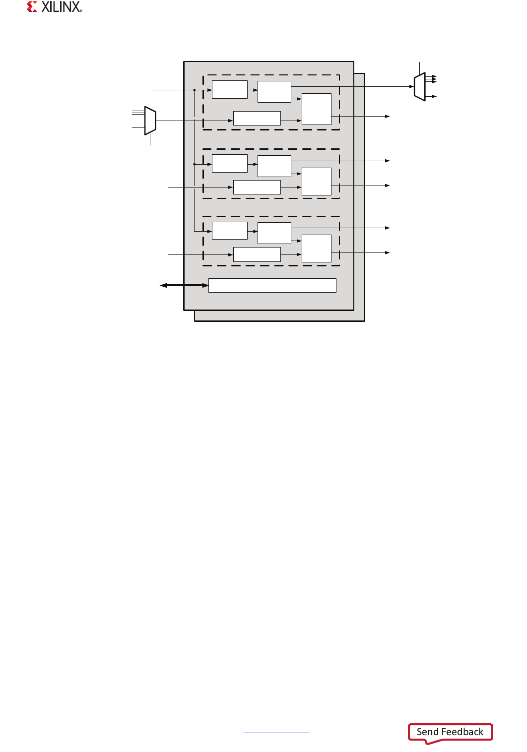
X-Ref Target - Figure 8-3
Figure 8-3: Triple Counter Timer Block Diagram
UG585_c8_08_120913
EMIO
Interface
Pre-scaler
TTC 0
16-bit
Counter
Event Timer
MIO
EMIO
CPU_1x
Interrupt
Timer/Clock 0
Wave-Out
Interrupt (GIC)
TTC_0: IRQ ID # 42
TTC_1: IRQ ID # 69
Pre-scaler
16-bit
Counter
Event Timer
Clock-In (EMIO)
Interrupt
Timer/Clock 1
Wave-Out (EMIO)
Pre-scaler
16-bit
Counter
Event Timer
Interrupt
Timer/Clock 2
TTC 1
MIO
EMIO
Wave-Out (EMIO)
Clock-In
Clock-In (EMIO)
APB
Status and Control Registers
Interrupt (GIC)
TTC_0: IRQ ID # 43
TTC_1: IRQ ID # 70
Interrupt (GIC)
TTC_0: IRQ ID # 44
TTC_1: IRQ ID # 71
slcr.MIO_PIN_xx.
slcr.MIO_PIN_xx