
User manual


Table Of Contents
- Zynq-7000 All Programmable SoC
- Table of Contents
- Ch. 1: Introduction
- Ch. 2: Signals, Interfaces, and Pins
- Ch. 3: Application Processing Unit
- Ch. 4: System Addresses
- Ch. 5: Interconnect
- Ch. 6: Boot and Configuration
- Ch. 7: Interrupts
- Ch. 8: Timers
- Ch. 9: DMA Controller
- Introduction
- Functional Description
- DMA Transfers on the AXI Interconnect
- AXI Transaction Considerations
- DMA Manager
- Multi-channel Data FIFO (MFIFO)
- Memory-to-Memory Transfers
- PL Peripheral AXI Transactions
- PL Peripheral Request Interface
- PL Peripheral - Length Managed by PL Peripheral
- PL Peripheral - Length Managed by DMAC
- Events and Interrupts
- Aborts
- Security
- IP Configuration Options
- Programming Guide for DMA Controller
- Programming Guide for DMA Engine
- Programming Restrictions
- System Functions
- I/O Interface
- Ch. 10: DDR Memory Controller
- Introduction
- AXI Memory Port Interface (DDRI)
- DDR Core and Transaction Scheduler (DDRC)
- DDRC Arbitration
- Controller PHY (DDRP)
- Initialization and Calibration
- DDR Clock Initialization
- DDR IOB Impedance Calibration
- DDR IOB Configuration
- DDR Controller Register Programming
- DRAM Reset and Initialization
- DRAM Input Impedance (ODT) Calibration
- DRAM Output Impedance (RON) Calibration
- DRAM Training
- Write Data Eye Adjustment
- Alternatives to Automatic DRAM Training
- DRAM Write Latency Restriction
- Register Overview
- Error Correction Code (ECC)
- Programming Model
- Ch. 11: Static Memory Controller
- Ch. 12: Quad-SPI Flash Controller
- Ch. 13: SD/SDIO Controller
- Ch. 14: General Purpose I/O (GPIO)
- Ch. 15: USB Host, Device, and OTG Controller
- Introduction
- Functional Description
- Programming Overview and Reference
- Device Mode Control
- Device Endpoint Data Structures
- Device Endpoint Packet Operational Model
- Device Endpoint Descriptor Reference
- Programming Guide for Device Controller
- Programming Guide for Device Endpoint Data Structures
- Host Mode Data Structures
- EHCI Implementation
- Host Data Structures Reference
- Programming Guide for Host Controller
- OTG Description and Reference
- System Functions
- I/O Interfaces
- Ch. 16: Gigabit Ethernet Controller
- Ch. 17: SPI Controller
- Ch. 18: CAN Controller
- Ch. 19: UART Controller
- Ch. 20: I2C Controller
- Ch. 21: Programmable Logic Description
- Ch. 22: Programmable Logic Design Guide
- Ch. 23: Programmable Logic Test and Debug
- Ch. 24: Power Management
- Ch. 25: Clocks
- Ch. 26: Reset System
- Ch. 27: JTAG and DAP Subsystem
- Ch. 28: System Test and Debug
- Ch. 29: On-Chip Memory (OCM)
- Ch. 30: XADC Interface
- Ch. 31: PCI Express
- Ch. 32: Device Secure Boot
- Appx. A: Additional Resources
- Appx. B: Register Details
- Overview
- Acronyms
- Module Summary
- AXI_HP Interface (AFI) (axi_hp)
- CAN Controller (can)
- DDR Memory Controller (ddrc)
- CoreSight Cross Trigger Interface (cti)
- Performance Monitor Unit (cortexa9_pmu)
- CoreSight Program Trace Macrocell (ptm)
- Debug Access Port (dap)
- CoreSight Embedded Trace Buffer (etb)
- PL Fabric Trace Monitor (ftm)
- CoreSight Trace Funnel (funnel)
- CoreSight Intstrumentation Trace Macrocell (itm)
- CoreSight Trace Packet Output (tpiu)
- Device Configuration Interface (devcfg)
- DMA Controller (dmac)
- Gigabit Ethernet Controller (GEM)
- General Purpose I/O (gpio)
- Interconnect QoS (qos301)
- NIC301 Address Region Control (nic301_addr_region_ctrl_registers)
- I2C Controller (IIC)
- L2 Cache (L2Cpl310)
- Application Processing Unit (mpcore)
- On-Chip Memory (ocm)
- Quad-SPI Flash Controller (qspi)
- SD Controller (sdio)
- System Level Control Registers (slcr)
- Static Memory Controller (pl353)
- SPI Controller (SPI)
- System Watchdog Timer (swdt)
- Triple Timer Counter (ttc)
- UART Controller (UART)
- USB Controller (usb)
Zynq-7000 AP SoC Technical Reference Manual www.xilinx.com 27
UG585 (v1.11) September 27, 2016
Chapter 1: Introduction
The processor(s) in the PS always boot first, allowing a software centric approach for PL system boot
and PL configuration. The PL can be configured as part of the boot process or configured at some
point in the future. Additionally, the PL can be completely reconfigured or used with partial, dynamic
reconfiguration (PR). PR allows configuration of a portion of the PL. This enables optional design
changes such as updating coefficients or time-multiplexing of the PL resources by swapping in new
algorithms as needed. This latter capability is analogous to the dynamic loading and unloading of
software modules. The PL configuration data is referred to as a bitstream.
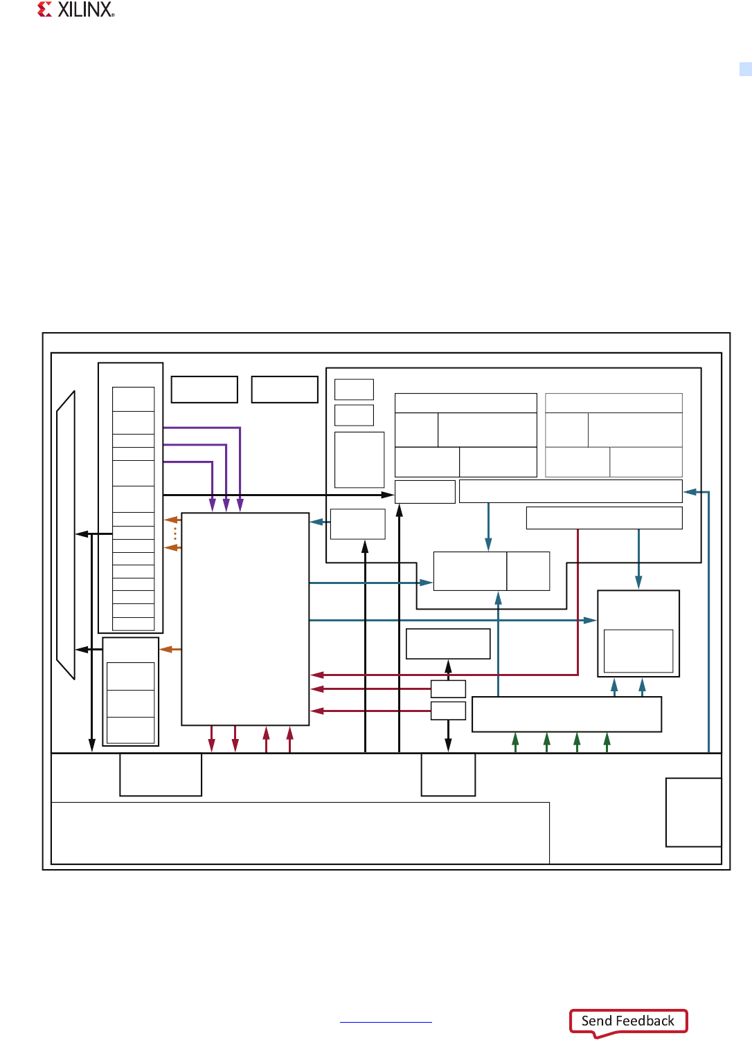
1.1.1 Block Diagram
Figure 1-1 illustrates the functional blocks of the Zynq-7000 AP SoC. The PS and the PL are on
separate power domains, enabling the user of these devices to power down the PL for power
management if required.
X-Ref Target - Figure 1-1
Figure 1-1: Zynq-7000 AP SoC Overview
2x USB
2x GigE
2x SD
Zynq-7000 AP SoC
I/O
Peripherals
IRQ
IRQ
EMIO
SelectIO
Resources
DMA 8
Channel
CoreSight
Components
Programmable Logic
DAP
DevC
SWDT
DMA
Sync
Notes:
1) Arrow direction shows control (master to slave)
2) Data flows in both directions: AXI 32bit/64bit, AXI 64bit, AXI 32bit, AHB 32bit, APB 32bit, Custom
3) Gray blocks in APU are applicable to dual core devices.
ACP
256K
SRAM
Application Processor Unit
TTC
System
Level
Control
Regs
GigE
CAN
SD
SDIO
UART
GPIO
UART
CAN
I2C
SRAM/
NOR
ONFI 1.0
NAND
Processing System
Memory
Interfaces
Q-SPI
CTRL
USB
GigE
I2C
USB
SD
SDIO
SPI
SPI
Programmable Logic to Memory
Interconnect
MMU
FPU and NEON Engine
Snoop Controller, AWDT, Timer
GIC
3
2 K
B
I-Cache
A
RM
C
ortex-A
9
C
P
U
ARM Cortex-A9
CPU
MMU
FPU and NEON En
g
in
e
Config
AES/
SHA
XADC
12 bit ADC
Memory
Interfaces
512 KB L2 Cache & Controller
OCM
Interconnect
DDR2/3,3L,
LPDDR2
Controller
UG585_c1_01_082216
3
2 K
B
D
-Cache
32 KB
I-Cache
32 KB
D-Cache
MIO
Clock
Generation
Reset
Central
Interconnect
General-Purpose
Ports
High-Performance Ports