
User manual


Table Of Contents
- Zynq-7000 All Programmable SoC
- Table of Contents
- Ch. 1: Introduction
- Ch. 2: Signals, Interfaces, and Pins
- Ch. 3: Application Processing Unit
- Ch. 4: System Addresses
- Ch. 5: Interconnect
- Ch. 6: Boot and Configuration
- Ch. 7: Interrupts
- Ch. 8: Timers
- Ch. 9: DMA Controller
- Introduction
- Functional Description
- DMA Transfers on the AXI Interconnect
- AXI Transaction Considerations
- DMA Manager
- Multi-channel Data FIFO (MFIFO)
- Memory-to-Memory Transfers
- PL Peripheral AXI Transactions
- PL Peripheral Request Interface
- PL Peripheral - Length Managed by PL Peripheral
- PL Peripheral - Length Managed by DMAC
- Events and Interrupts
- Aborts
- Security
- IP Configuration Options
- Programming Guide for DMA Controller
- Programming Guide for DMA Engine
- Programming Restrictions
- System Functions
- I/O Interface
- Ch. 10: DDR Memory Controller
- Introduction
- AXI Memory Port Interface (DDRI)
- DDR Core and Transaction Scheduler (DDRC)
- DDRC Arbitration
- Controller PHY (DDRP)
- Initialization and Calibration
- DDR Clock Initialization
- DDR IOB Impedance Calibration
- DDR IOB Configuration
- DDR Controller Register Programming
- DRAM Reset and Initialization
- DRAM Input Impedance (ODT) Calibration
- DRAM Output Impedance (RON) Calibration
- DRAM Training
- Write Data Eye Adjustment
- Alternatives to Automatic DRAM Training
- DRAM Write Latency Restriction
- Register Overview
- Error Correction Code (ECC)
- Programming Model
- Ch. 11: Static Memory Controller
- Ch. 12: Quad-SPI Flash Controller
- Ch. 13: SD/SDIO Controller
- Ch. 14: General Purpose I/O (GPIO)
- Ch. 15: USB Host, Device, and OTG Controller
- Introduction
- Functional Description
- Programming Overview and Reference
- Device Mode Control
- Device Endpoint Data Structures
- Device Endpoint Packet Operational Model
- Device Endpoint Descriptor Reference
- Programming Guide for Device Controller
- Programming Guide for Device Endpoint Data Structures
- Host Mode Data Structures
- EHCI Implementation
- Host Data Structures Reference
- Programming Guide for Host Controller
- OTG Description and Reference
- System Functions
- I/O Interfaces
- Ch. 16: Gigabit Ethernet Controller
- Ch. 17: SPI Controller
- Ch. 18: CAN Controller
- Ch. 19: UART Controller
- Ch. 20: I2C Controller
- Ch. 21: Programmable Logic Description
- Ch. 22: Programmable Logic Design Guide
- Ch. 23: Programmable Logic Test and Debug
- Ch. 24: Power Management
- Ch. 25: Clocks
- Ch. 26: Reset System
- Ch. 27: JTAG and DAP Subsystem
- Ch. 28: System Test and Debug
- Ch. 29: On-Chip Memory (OCM)
- Ch. 30: XADC Interface
- Ch. 31: PCI Express
- Ch. 32: Device Secure Boot
- Appx. A: Additional Resources
- Appx. B: Register Details
- Overview
- Acronyms
- Module Summary
- AXI_HP Interface (AFI) (axi_hp)
- CAN Controller (can)
- DDR Memory Controller (ddrc)
- CoreSight Cross Trigger Interface (cti)
- Performance Monitor Unit (cortexa9_pmu)
- CoreSight Program Trace Macrocell (ptm)
- Debug Access Port (dap)
- CoreSight Embedded Trace Buffer (etb)
- PL Fabric Trace Monitor (ftm)
- CoreSight Trace Funnel (funnel)
- CoreSight Intstrumentation Trace Macrocell (itm)
- CoreSight Trace Packet Output (tpiu)
- Device Configuration Interface (devcfg)
- DMA Controller (dmac)
- Gigabit Ethernet Controller (GEM)
- General Purpose I/O (gpio)
- Interconnect QoS (qos301)
- NIC301 Address Region Control (nic301_addr_region_ctrl_registers)
- I2C Controller (IIC)
- L2 Cache (L2Cpl310)
- Application Processing Unit (mpcore)
- On-Chip Memory (ocm)
- Quad-SPI Flash Controller (qspi)
- SD Controller (sdio)
- System Level Control Registers (slcr)
- Static Memory Controller (pl353)
- SPI Controller (SPI)
- System Watchdog Timer (swdt)
- Triple Timer Counter (ttc)
- UART Controller (UART)
- USB Controller (usb)
Zynq-7000 AP SoC Technical Reference Manual www.xilinx.com 28
UG585 (v1.11) September 27, 2016
Chapter 1: Introduction
The Zynq-7000 AP SoC is composed of the following major functional blocks:
• Processing System (PS)
°
Application processor unit (APU)
°
Memory interfaces
°
I/O peripherals (IOP)
°
Interconnect
• Programmable Logic (PL)
1.1.2 Documentation Resources
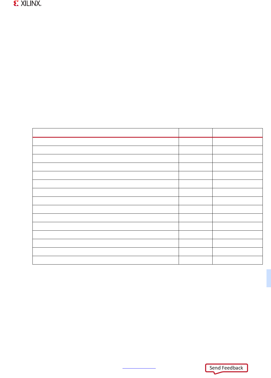
Table 1-1 identifies the versions of third-party IP used in the Zynq-7000 AP SoC devices.
The PL is derived from Xilinx 7 series FPGA technology: Artix®-7 for the 7z010/7z015/7z020 (dual
core devices) and 7z007s/7z012s/7z014s (single core devices), and Kintex®-7 for the
7z030/7z035/7z045/7z100 devices. The PL is used to extend the functionality to meet specific
application requirements. The PL includes many different types of resources including configurable
logic blocks (CLBs), port and width configurable block RAM (BRAM), DSP slices with a 25 x 18
multiplier, 48-bit accumulator and pre-adder (DSP48E1), a user configurable analog to digital
convertor (XADC), clock management tiles (CMT), a configuration block with 256b AES for
decryption and SHA for authentication, configurable SelectIO™ technology and optionally GTP or
GTX multi-gigabit transceivers and an integrated PCI Express® (PCIe) block.
Table 1-1: Vendor IP Versions
Unit Supplier Version
Cortex-A9 MPCore ARM r3p0
AMBA Level 2 Cache Controller (PL310) ARM r3p2-50rel0
PrimeCell Static Memory Controller (PL353) ARM r2p1
PrimeCell DMA Controller (PL330) ARM r1p1
Generic Interrupt Controller (PL390) ARM Arch v1.0, r0p0
CoreLink Network Interconnect (NIC-301) ARM r2p2
DesignWare Cores IntelliDDR Multi Protocol Memory Controller Synopsys A07
USB 2.0 High Speed Atlantic Controller Synopsys 2.20a
Watchdog Timer Cadence Rev 07
Inter Intergrated Circuit Cadence r1p10
Gigabit Ethernet MAC Cadence r1p23
Serial Peripheral Interface Cadence r1p06
Universal Asynchronous Receiver Transmitter Cadence r1p08
Triple Timer Counter Cadence Rev 06
SD2.0/SDIO2.0/MMC3.31 AHB Host Controller Arasan 8.9A_apr02nd_2010