
User manual


Table Of Contents
- Zynq-7000 All Programmable SoC
- Table of Contents
- Ch. 1: Introduction
- Ch. 2: Signals, Interfaces, and Pins
- Ch. 3: Application Processing Unit
- Ch. 4: System Addresses
- Ch. 5: Interconnect
- Ch. 6: Boot and Configuration
- Ch. 7: Interrupts
- Ch. 8: Timers
- Ch. 9: DMA Controller
- Introduction
- Functional Description
- DMA Transfers on the AXI Interconnect
- AXI Transaction Considerations
- DMA Manager
- Multi-channel Data FIFO (MFIFO)
- Memory-to-Memory Transfers
- PL Peripheral AXI Transactions
- PL Peripheral Request Interface
- PL Peripheral - Length Managed by PL Peripheral
- PL Peripheral - Length Managed by DMAC
- Events and Interrupts
- Aborts
- Security
- IP Configuration Options
- Programming Guide for DMA Controller
- Programming Guide for DMA Engine
- Programming Restrictions
- System Functions
- I/O Interface
- Ch. 10: DDR Memory Controller
- Introduction
- AXI Memory Port Interface (DDRI)
- DDR Core and Transaction Scheduler (DDRC)
- DDRC Arbitration
- Controller PHY (DDRP)
- Initialization and Calibration
- DDR Clock Initialization
- DDR IOB Impedance Calibration
- DDR IOB Configuration
- DDR Controller Register Programming
- DRAM Reset and Initialization
- DRAM Input Impedance (ODT) Calibration
- DRAM Output Impedance (RON) Calibration
- DRAM Training
- Write Data Eye Adjustment
- Alternatives to Automatic DRAM Training
- DRAM Write Latency Restriction
- Register Overview
- Error Correction Code (ECC)
- Programming Model
- Ch. 11: Static Memory Controller
- Ch. 12: Quad-SPI Flash Controller
- Ch. 13: SD/SDIO Controller
- Ch. 14: General Purpose I/O (GPIO)
- Ch. 15: USB Host, Device, and OTG Controller
- Introduction
- Functional Description
- Programming Overview and Reference
- Device Mode Control
- Device Endpoint Data Structures
- Device Endpoint Packet Operational Model
- Device Endpoint Descriptor Reference
- Programming Guide for Device Controller
- Programming Guide for Device Endpoint Data Structures
- Host Mode Data Structures
- EHCI Implementation
- Host Data Structures Reference
- Programming Guide for Host Controller
- OTG Description and Reference
- System Functions
- I/O Interfaces
- Ch. 16: Gigabit Ethernet Controller
- Ch. 17: SPI Controller
- Ch. 18: CAN Controller
- Ch. 19: UART Controller
- Ch. 20: I2C Controller
- Ch. 21: Programmable Logic Description
- Ch. 22: Programmable Logic Design Guide
- Ch. 23: Programmable Logic Test and Debug
- Ch. 24: Power Management
- Ch. 25: Clocks
- Ch. 26: Reset System
- Ch. 27: JTAG and DAP Subsystem
- Ch. 28: System Test and Debug
- Ch. 29: On-Chip Memory (OCM)
- Ch. 30: XADC Interface
- Ch. 31: PCI Express
- Ch. 32: Device Secure Boot
- Appx. A: Additional Resources
- Appx. B: Register Details
- Overview
- Acronyms
- Module Summary
- AXI_HP Interface (AFI) (axi_hp)
- CAN Controller (can)
- DDR Memory Controller (ddrc)
- CoreSight Cross Trigger Interface (cti)
- Performance Monitor Unit (cortexa9_pmu)
- CoreSight Program Trace Macrocell (ptm)
- Debug Access Port (dap)
- CoreSight Embedded Trace Buffer (etb)
- PL Fabric Trace Monitor (ftm)
- CoreSight Trace Funnel (funnel)
- CoreSight Intstrumentation Trace Macrocell (itm)
- CoreSight Trace Packet Output (tpiu)
- Device Configuration Interface (devcfg)
- DMA Controller (dmac)
- Gigabit Ethernet Controller (GEM)
- General Purpose I/O (gpio)
- Interconnect QoS (qos301)
- NIC301 Address Region Control (nic301_addr_region_ctrl_registers)
- I2C Controller (IIC)
- L2 Cache (L2Cpl310)
- Application Processing Unit (mpcore)
- On-Chip Memory (ocm)
- Quad-SPI Flash Controller (qspi)
- SD Controller (sdio)
- System Level Control Registers (slcr)
- Static Memory Controller (pl353)
- SPI Controller (SPI)
- System Watchdog Timer (swdt)
- Triple Timer Counter (ttc)
- UART Controller (UART)
- USB Controller (usb)
Zynq-7000 AP SoC Technical Reference Manual www.xilinx.com 295
UG585 (v1.11) September 27, 2016
Chapter 10: DDR Memory Controller
• slcr.DDRIOB_DRIVE_SLEW_DATA
• slcr.DDRIOB_DRIVE_SLEW_DIFF
• slcr.DDRIOB_DRIVE_SLEW_CLOCK
The input Vref settings are controlled by slcr.DDRIOB_DDR_CTRL. The DDR DCI settings are
controlled by slcr.DDRIOB_DCI_CTRL.
Note: The 7z010 dual core and 7z007s single core CLG225 devices only support a 16-bit data bus
width, not a 32-bit bus width.
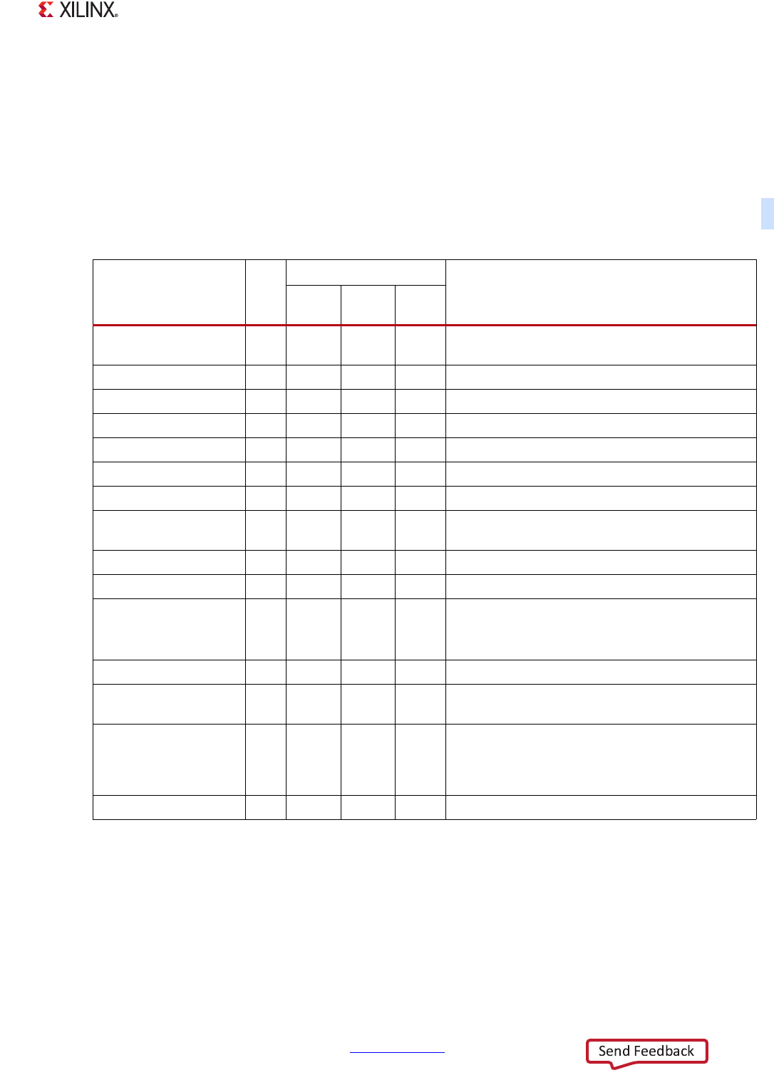
Table 10-3: DDR I/O Signal Pin List
Device Pin Name I/O
Connections
Description
DDR2 LPDDR2
DDR3/
DDR3L
PS_DDR_CKP
PS_DDR_CKN
O X X X Differential clock outputs
PS_DDR_CKE O X X X Clock enable
PS_DDR_CS_B O X X X Chip select
PS_DDR_RAS_B O X X RAS row address strobe
PS_DDR_CAS_B O X X RAS column address strobe
PS_DDR_WE_B O X X Write enable
PS_DDR_BA[2:0] O X X Bank address
PS_DDR_A[14:0] O
XXX
DDR3/DDR3L/DDR2: Row/Column Address
LPDDR2: CA[9:0] = DDR_A[9:0]
PS_DDR_ODT O X X Output dynamic termination signal
PS_DDR_DRST_B O X Reset
PS_DDR_DQ[31:0] IO X X X
32-bit Data bus: [31:0]
16-bit Data bus: [15:0]
16-bit Data with ECC
PS_DDR_DM[3:0] O X X X Data byte masks
PS_DDR_DQS_P[3:0]
PS_DDR_DQS_N[3:0]
IO X X X Differential data strobes
PS_DDR_VR{P,N} ~ X X X
DCI voltage reference. Used to calibrate input
termination. and DDR I/O drive strength. Connect
DDR_VRP to a resistor to GND. Connect DDR_VRN
to a resister to VCC_DDR.
PS_DDR_VREF[1:0] ~ X X X Voltage reference