
User manual


Table Of Contents
- Zynq-7000 All Programmable SoC
- Table of Contents
- Ch. 1: Introduction
- Ch. 2: Signals, Interfaces, and Pins
- Ch. 3: Application Processing Unit
- Ch. 4: System Addresses
- Ch. 5: Interconnect
- Ch. 6: Boot and Configuration
- Ch. 7: Interrupts
- Ch. 8: Timers
- Ch. 9: DMA Controller
- Introduction
- Functional Description
- DMA Transfers on the AXI Interconnect
- AXI Transaction Considerations
- DMA Manager
- Multi-channel Data FIFO (MFIFO)
- Memory-to-Memory Transfers
- PL Peripheral AXI Transactions
- PL Peripheral Request Interface
- PL Peripheral - Length Managed by PL Peripheral
- PL Peripheral - Length Managed by DMAC
- Events and Interrupts
- Aborts
- Security
- IP Configuration Options
- Programming Guide for DMA Controller
- Programming Guide for DMA Engine
- Programming Restrictions
- System Functions
- I/O Interface
- Ch. 10: DDR Memory Controller
- Introduction
- AXI Memory Port Interface (DDRI)
- DDR Core and Transaction Scheduler (DDRC)
- DDRC Arbitration
- Controller PHY (DDRP)
- Initialization and Calibration
- DDR Clock Initialization
- DDR IOB Impedance Calibration
- DDR IOB Configuration
- DDR Controller Register Programming
- DRAM Reset and Initialization
- DRAM Input Impedance (ODT) Calibration
- DRAM Output Impedance (RON) Calibration
- DRAM Training
- Write Data Eye Adjustment
- Alternatives to Automatic DRAM Training
- DRAM Write Latency Restriction
- Register Overview
- Error Correction Code (ECC)
- Programming Model
- Ch. 11: Static Memory Controller
- Ch. 12: Quad-SPI Flash Controller
- Ch. 13: SD/SDIO Controller
- Ch. 14: General Purpose I/O (GPIO)
- Ch. 15: USB Host, Device, and OTG Controller
- Introduction
- Functional Description
- Programming Overview and Reference
- Device Mode Control
- Device Endpoint Data Structures
- Device Endpoint Packet Operational Model
- Device Endpoint Descriptor Reference
- Programming Guide for Device Controller
- Programming Guide for Device Endpoint Data Structures
- Host Mode Data Structures
- EHCI Implementation
- Host Data Structures Reference
- Programming Guide for Host Controller
- OTG Description and Reference
- System Functions
- I/O Interfaces
- Ch. 16: Gigabit Ethernet Controller
- Ch. 17: SPI Controller
- Ch. 18: CAN Controller
- Ch. 19: UART Controller
- Ch. 20: I2C Controller
- Ch. 21: Programmable Logic Description
- Ch. 22: Programmable Logic Design Guide
- Ch. 23: Programmable Logic Test and Debug
- Ch. 24: Power Management
- Ch. 25: Clocks
- Ch. 26: Reset System
- Ch. 27: JTAG and DAP Subsystem
- Ch. 28: System Test and Debug
- Ch. 29: On-Chip Memory (OCM)
- Ch. 30: XADC Interface
- Ch. 31: PCI Express
- Ch. 32: Device Secure Boot
- Appx. A: Additional Resources
- Appx. B: Register Details
- Overview
- Acronyms
- Module Summary
- AXI_HP Interface (AFI) (axi_hp)
- CAN Controller (can)
- DDR Memory Controller (ddrc)
- CoreSight Cross Trigger Interface (cti)
- Performance Monitor Unit (cortexa9_pmu)
- CoreSight Program Trace Macrocell (ptm)
- Debug Access Port (dap)
- CoreSight Embedded Trace Buffer (etb)
- PL Fabric Trace Monitor (ftm)
- CoreSight Trace Funnel (funnel)
- CoreSight Intstrumentation Trace Macrocell (itm)
- CoreSight Trace Packet Output (tpiu)
- Device Configuration Interface (devcfg)
- DMA Controller (dmac)
- Gigabit Ethernet Controller (GEM)
- General Purpose I/O (gpio)
- Interconnect QoS (qos301)
- NIC301 Address Region Control (nic301_addr_region_ctrl_registers)
- I2C Controller (IIC)
- L2 Cache (L2Cpl310)
- Application Processing Unit (mpcore)
- On-Chip Memory (ocm)
- Quad-SPI Flash Controller (qspi)
- SD Controller (sdio)
- System Level Control Registers (slcr)
- Static Memory Controller (pl353)
- SPI Controller (SPI)
- System Watchdog Timer (swdt)
- Triple Timer Counter (ttc)
- UART Controller (UART)
- USB Controller (usb)
Zynq-7000 AP SoC Technical Reference Manual www.xilinx.com 310
UG585 (v1.11) September 27, 2016
Chapter 10: DDR Memory Controller
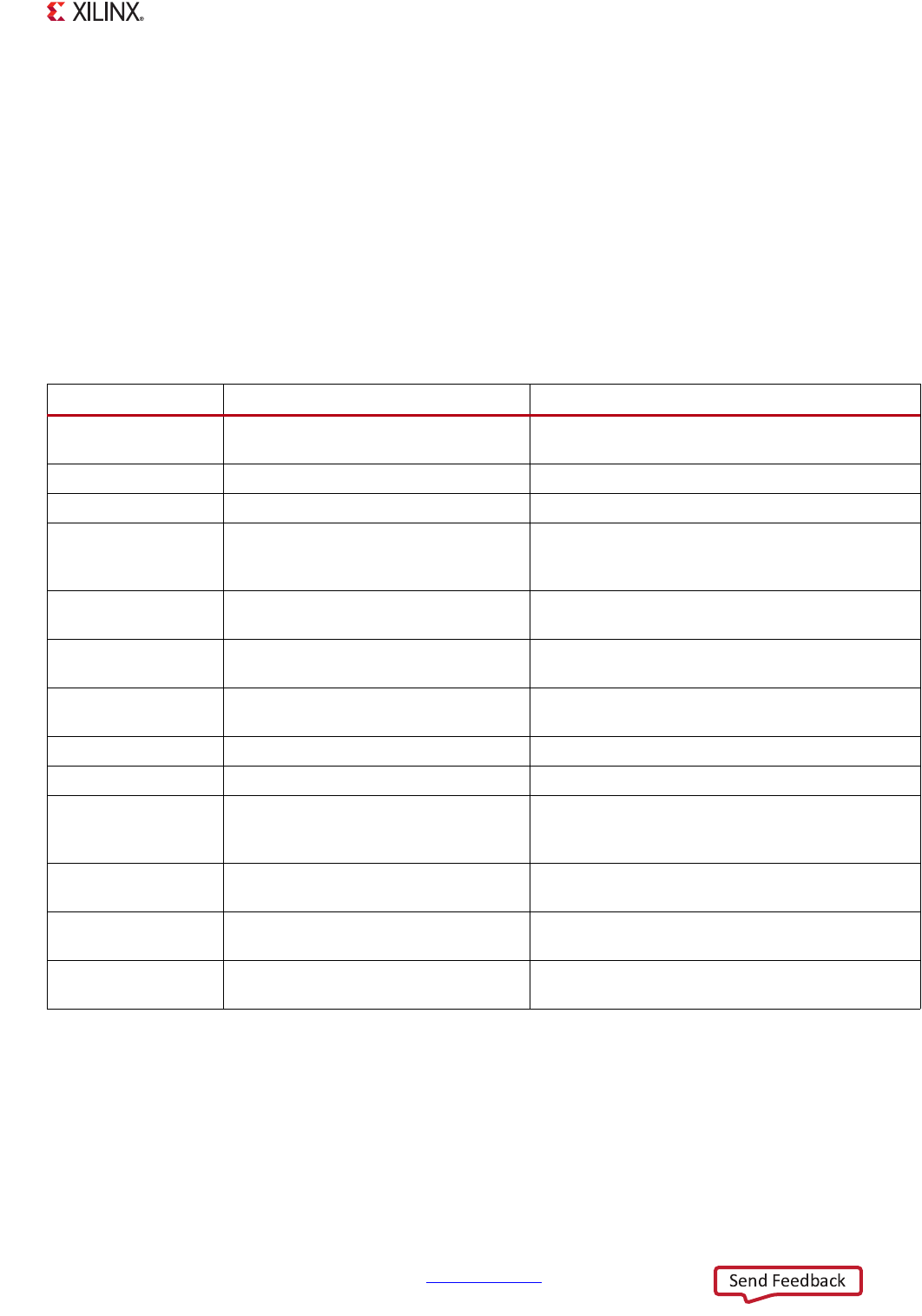
10.6.3 DDR IOB Configuration
The DDR IOBs must be configured to function as I/O. Each type of DDR IOB is controlled by two
different SLCR configuration registers. The configuration registers configure the IOB's input mode,
output mode, DCI mode, and other functions.
Configuration
The DDR system supports DDR3L/DDR3/DDR2/LPDDR2 in 16 and 32 bit modes and power down
modes. The registers identified in Table 10-8 control groups of I/Os and must be configured
depending on the particular mode.
Set the IOB configuration as follows:
1. Set DCI_TYPE to DCI Drive for all LPDDR2 I/Os.
2. Set DCI_TYPE to DCI Termination for DDR2/DDR3/DDR3L bidirectional I/Os.
3. Set OUTPUT_EN = obuf to enable outputs.
Table 10-8: DDR IOB Configuration Registers
Register Affected I/O Blocks Description
DDRIOB_DDR_CTRL VREF, VRN, VRP, DRST Controls special I/O modes for internal and external
VREF and DCI reference pins VRN and VRP
DDRIOB_DCI_CTRL DCI controller Enables the DCI controller
DDRIOB_DCI_STATUS DCI controller Status for the DCI controller
DDRIOB_ADDR0
DDRIOB_ADDR1
DDR_A[14:0], DDR_CKE, DDR_BA[2:0],
DDR_ODT, DDR_WE_B, DDR_CAS_B,
DDR_RAS_B DDR_CS_B
Configuration settings for address and control
outputs used by LPDDR2, DDR2 and DDR3/DDR3L
DDRIOB_CLOCK DDR_CK_P, DDR_CK_P Configuration settings for the differential clock
outputs. Controls DDR_CK_P, DDR_CK_P
DDRIOB_DATA0 DDR_DQ[15:0], DDR_DM[1:0],
DDR_FIFO_IN[0], DDR_FIFO_OUT[0]
Configuration settings for data and mask bits for
lower 16-bits
DDRIOB_DATA1 DDR_DQ[31:16], DDR_DM[3:2],
DDR_FIFO_IN[1], DDR_FIFO_OUT[1]
Configuration settings for data and mask bits for
upper16-bits
DDRIOB_DIFF0 DDR_DQS_P[1:0], DDR_DQS_N[1:0] Configuration settings for dqs bits for lower 16-bits
DDRIOB_DIFF1 DDR_DQS_P[3:2], DDR_DQS_N[3:2] Configuration settings for dqs bits for upper 16-bits
DDRIOB_DRIVE_SLEW
_ADDR
DDR_A[14:0], DDR_CKE, DDR_BA[2:0],
DDR_ODT, DDR_WE_B, DDR_CAS_B,
DDR_RAS_B, DDR_CS_B
Drive strength and slew rate settings for address
and control output
DDRIOB_DRIVE_SLEW
_CLOCK
DDR_CK_P, DDR_CK_P Drive strength and slew rate settings for the clock
outputs
DDRIOB_DRIVE_SLEW
_DATA
DDR_DQ[31:0], DDR_DM[3:0],
DDR_FIFO_IN[1:0], DDR_FIFO_OUT[1:0]
Drive strength and slew rate settings for data I/Os
DDRIOB_DRIVE_SLEW
_DIFF
DDR_DQS_P[3:0], DDR_DQS_N[3:2] Drive strength and slew rate settings for data strobe
I/Os