
User manual


Table Of Contents
- Zynq-7000 All Programmable SoC
- Table of Contents
- Ch. 1: Introduction
- Ch. 2: Signals, Interfaces, and Pins
- Ch. 3: Application Processing Unit
- Ch. 4: System Addresses
- Ch. 5: Interconnect
- Ch. 6: Boot and Configuration
- Ch. 7: Interrupts
- Ch. 8: Timers
- Ch. 9: DMA Controller
- Introduction
- Functional Description
- DMA Transfers on the AXI Interconnect
- AXI Transaction Considerations
- DMA Manager
- Multi-channel Data FIFO (MFIFO)
- Memory-to-Memory Transfers
- PL Peripheral AXI Transactions
- PL Peripheral Request Interface
- PL Peripheral - Length Managed by PL Peripheral
- PL Peripheral - Length Managed by DMAC
- Events and Interrupts
- Aborts
- Security
- IP Configuration Options
- Programming Guide for DMA Controller
- Programming Guide for DMA Engine
- Programming Restrictions
- System Functions
- I/O Interface
- Ch. 10: DDR Memory Controller
- Introduction
- AXI Memory Port Interface (DDRI)
- DDR Core and Transaction Scheduler (DDRC)
- DDRC Arbitration
- Controller PHY (DDRP)
- Initialization and Calibration
- DDR Clock Initialization
- DDR IOB Impedance Calibration
- DDR IOB Configuration
- DDR Controller Register Programming
- DRAM Reset and Initialization
- DRAM Input Impedance (ODT) Calibration
- DRAM Output Impedance (RON) Calibration
- DRAM Training
- Write Data Eye Adjustment
- Alternatives to Automatic DRAM Training
- DRAM Write Latency Restriction
- Register Overview
- Error Correction Code (ECC)
- Programming Model
- Ch. 11: Static Memory Controller
- Ch. 12: Quad-SPI Flash Controller
- Ch. 13: SD/SDIO Controller
- Ch. 14: General Purpose I/O (GPIO)
- Ch. 15: USB Host, Device, and OTG Controller
- Introduction
- Functional Description
- Programming Overview and Reference
- Device Mode Control
- Device Endpoint Data Structures
- Device Endpoint Packet Operational Model
- Device Endpoint Descriptor Reference
- Programming Guide for Device Controller
- Programming Guide for Device Endpoint Data Structures
- Host Mode Data Structures
- EHCI Implementation
- Host Data Structures Reference
- Programming Guide for Host Controller
- OTG Description and Reference
- System Functions
- I/O Interfaces
- Ch. 16: Gigabit Ethernet Controller
- Ch. 17: SPI Controller
- Ch. 18: CAN Controller
- Ch. 19: UART Controller
- Ch. 20: I2C Controller
- Ch. 21: Programmable Logic Description
- Ch. 22: Programmable Logic Design Guide
- Ch. 23: Programmable Logic Test and Debug
- Ch. 24: Power Management
- Ch. 25: Clocks
- Ch. 26: Reset System
- Ch. 27: JTAG and DAP Subsystem
- Ch. 28: System Test and Debug
- Ch. 29: On-Chip Memory (OCM)
- Ch. 30: XADC Interface
- Ch. 31: PCI Express
- Ch. 32: Device Secure Boot
- Appx. A: Additional Resources
- Appx. B: Register Details
- Overview
- Acronyms
- Module Summary
- AXI_HP Interface (AFI) (axi_hp)
- CAN Controller (can)
- DDR Memory Controller (ddrc)
- CoreSight Cross Trigger Interface (cti)
- Performance Monitor Unit (cortexa9_pmu)
- CoreSight Program Trace Macrocell (ptm)
- Debug Access Port (dap)
- CoreSight Embedded Trace Buffer (etb)
- PL Fabric Trace Monitor (ftm)
- CoreSight Trace Funnel (funnel)
- CoreSight Intstrumentation Trace Macrocell (itm)
- CoreSight Trace Packet Output (tpiu)
- Device Configuration Interface (devcfg)
- DMA Controller (dmac)
- Gigabit Ethernet Controller (GEM)
- General Purpose I/O (gpio)
- Interconnect QoS (qos301)
- NIC301 Address Region Control (nic301_addr_region_ctrl_registers)
- I2C Controller (IIC)
- L2 Cache (L2Cpl310)
- Application Processing Unit (mpcore)
- On-Chip Memory (ocm)
- Quad-SPI Flash Controller (qspi)
- SD Controller (sdio)
- System Level Control Registers (slcr)
- Static Memory Controller (pl353)
- SPI Controller (SPI)
- System Watchdog Timer (swdt)
- Triple Timer Counter (ttc)
- UART Controller (UART)
- USB Controller (usb)
Zynq-7000 AP SoC Technical Reference Manual www.xilinx.com 322
UG585 (v1.11) September 27, 2016
Chapter 10: DDR Memory Controller
10.8 Error Correction Code (ECC)
There is optional ECC support in half-bus width (16-bit) data width configuration only.
Externally 26 bits of a DRAM DDR device are required, 16-bits for data and 10 bits for ECC. Each data
byte uses an independent 5-bit ECC field. This mode provides single error correction and dual error
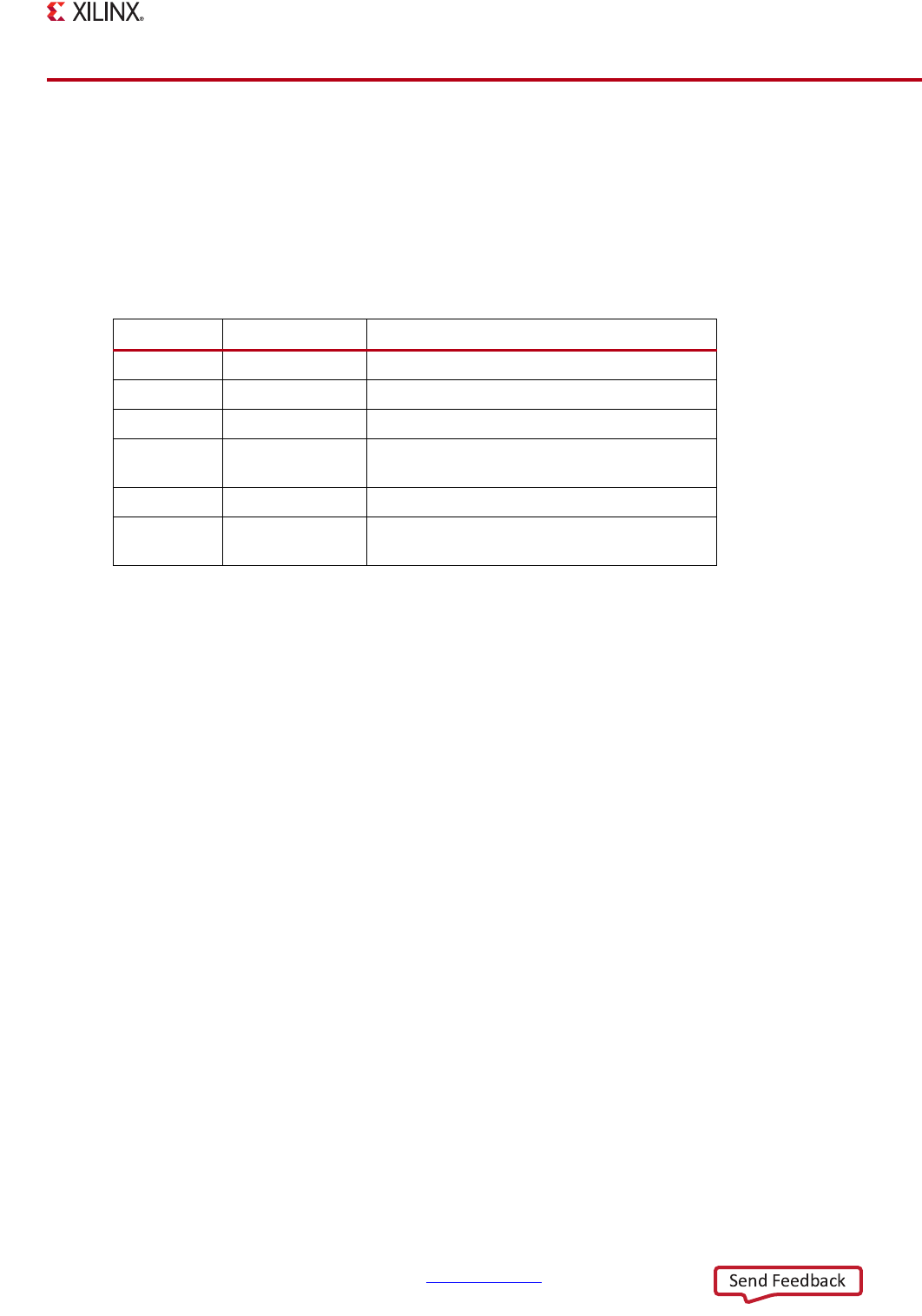
detection. The ECC bits are interlaced with the data bits and unused bits as shown in Table 10-13.
10.8.1 ECC Initialization
ECC is supported in 16-bit bus mode only. When enabled, a write operation computes and stores an
ECC code along with the data, and a read operation reads and checks the data against the stored ECC
code. It is therefore possible to receive ECC errors when reading uninitialized memory locations. To
avoid this problem, all memory locations must be written before being read. Note that, since ECC is
computed and checked over a byte resolution, a read of 1 byte is done to a 16-bit location that has
only that byte initialized (second byte of 16-bit location is uninitialized) does not result in an ECC
error. The controller only checks ECC on the byte that has been read. Writing to the entire DDR DRAM
through the CPU can be time intensive. It may be worthwhile to use a DMA device to generate larger
bursts to the DDR controller initialization and offload the CPU. Note that only the ARM CPU and ACP
interfaces can access the lowest 512 KB of DDR (see Table 4-1), CPU software may still need to
initialize this region of ECC-based DDR.
Note that while only two data byte lanes are used for actual data, all four lanes are used in ECC mode,
and therefore DDR training must be performed on all lanes.
10.8.2 ECC Error Behavior
For correctable ECC errors, there is no error actively signaled via an interrupt or AXI response.
For uncorrectable ECC errors, the controller returns a SLVERR response back to the re-questing AXI
bus master. In both cases, information regarding the error (such as column, row and bank error
address, error byte lane, etc.) is logged in the controller register space.
When the controller detects a correctable ECC error, it does the following:
Table 10-13: ECC Data Bit Assignments
DRAM DQ pin Number of Pins Function
DQ[7:0] 8 First Data Byte
DQ[15:8] 8 Second Data Byte
DQ[20:16] 5 ECC bits associated with first Data Byte
DQ[23:21] 3 Unused bits. Connect to DRAM for proper
initialization purpose
DQ[28:24] 5 ECC bits associated with second Data Byte
DQ[31:29] 3 Unused bits. Connect to DRAM for proper
initialization purpose