
User manual


Table Of Contents
- Zynq-7000 All Programmable SoC
- Table of Contents
- Ch. 1: Introduction
- Ch. 2: Signals, Interfaces, and Pins
- Ch. 3: Application Processing Unit
- Ch. 4: System Addresses
- Ch. 5: Interconnect
- Ch. 6: Boot and Configuration
- Ch. 7: Interrupts
- Ch. 8: Timers
- Ch. 9: DMA Controller
- Introduction
- Functional Description
- DMA Transfers on the AXI Interconnect
- AXI Transaction Considerations
- DMA Manager
- Multi-channel Data FIFO (MFIFO)
- Memory-to-Memory Transfers
- PL Peripheral AXI Transactions
- PL Peripheral Request Interface
- PL Peripheral - Length Managed by PL Peripheral
- PL Peripheral - Length Managed by DMAC
- Events and Interrupts
- Aborts
- Security
- IP Configuration Options
- Programming Guide for DMA Controller
- Programming Guide for DMA Engine
- Programming Restrictions
- System Functions
- I/O Interface
- Ch. 10: DDR Memory Controller
- Introduction
- AXI Memory Port Interface (DDRI)
- DDR Core and Transaction Scheduler (DDRC)
- DDRC Arbitration
- Controller PHY (DDRP)
- Initialization and Calibration
- DDR Clock Initialization
- DDR IOB Impedance Calibration
- DDR IOB Configuration
- DDR Controller Register Programming
- DRAM Reset and Initialization
- DRAM Input Impedance (ODT) Calibration
- DRAM Output Impedance (RON) Calibration
- DRAM Training
- Write Data Eye Adjustment
- Alternatives to Automatic DRAM Training
- DRAM Write Latency Restriction
- Register Overview
- Error Correction Code (ECC)
- Programming Model
- Ch. 11: Static Memory Controller
- Ch. 12: Quad-SPI Flash Controller
- Ch. 13: SD/SDIO Controller
- Ch. 14: General Purpose I/O (GPIO)
- Ch. 15: USB Host, Device, and OTG Controller
- Introduction
- Functional Description
- Programming Overview and Reference
- Device Mode Control
- Device Endpoint Data Structures
- Device Endpoint Packet Operational Model
- Device Endpoint Descriptor Reference
- Programming Guide for Device Controller
- Programming Guide for Device Endpoint Data Structures
- Host Mode Data Structures
- EHCI Implementation
- Host Data Structures Reference
- Programming Guide for Host Controller
- OTG Description and Reference
- System Functions
- I/O Interfaces
- Ch. 16: Gigabit Ethernet Controller
- Ch. 17: SPI Controller
- Ch. 18: CAN Controller
- Ch. 19: UART Controller
- Ch. 20: I2C Controller
- Ch. 21: Programmable Logic Description
- Ch. 22: Programmable Logic Design Guide
- Ch. 23: Programmable Logic Test and Debug
- Ch. 24: Power Management
- Ch. 25: Clocks
- Ch. 26: Reset System
- Ch. 27: JTAG and DAP Subsystem
- Ch. 28: System Test and Debug
- Ch. 29: On-Chip Memory (OCM)
- Ch. 30: XADC Interface
- Ch. 31: PCI Express
- Ch. 32: Device Secure Boot
- Appx. A: Additional Resources
- Appx. B: Register Details
- Overview
- Acronyms
- Module Summary
- AXI_HP Interface (AFI) (axi_hp)
- CAN Controller (can)
- DDR Memory Controller (ddrc)
- CoreSight Cross Trigger Interface (cti)
- Performance Monitor Unit (cortexa9_pmu)
- CoreSight Program Trace Macrocell (ptm)
- Debug Access Port (dap)
- CoreSight Embedded Trace Buffer (etb)
- PL Fabric Trace Monitor (ftm)
- CoreSight Trace Funnel (funnel)
- CoreSight Intstrumentation Trace Macrocell (itm)
- CoreSight Trace Packet Output (tpiu)
- Device Configuration Interface (devcfg)
- DMA Controller (dmac)
- Gigabit Ethernet Controller (GEM)
- General Purpose I/O (gpio)
- Interconnect QoS (qos301)
- NIC301 Address Region Control (nic301_addr_region_ctrl_registers)
- I2C Controller (IIC)
- L2 Cache (L2Cpl310)
- Application Processing Unit (mpcore)
- On-Chip Memory (ocm)
- Quad-SPI Flash Controller (qspi)
- SD Controller (sdio)
- System Level Control Registers (slcr)
- Static Memory Controller (pl353)
- SPI Controller (SPI)
- System Watchdog Timer (swdt)
- Triple Timer Counter (ttc)
- UART Controller (UART)
- USB Controller (usb)
Zynq-7000 AP SoC Technical Reference Manual www.xilinx.com 330
UG585 (v1.11) September 27, 2016
Chapter 11: Static Memory Controller
11.1.3 Notices
7z007s and 7z010 CLG225 Devices
The 7z007s single core 7z010 dual core CLG225 devices do not support the NOR/SRAM interface.
The NAND interface is supported in the 8-bit interface, but not the 16-bit interface.
MIO Pin Options
MIO Pin 1 can be programmed to be CS1 or address bit 25 for the NOR/SRAM controller. This pin can
also be programmed as a GPIO. Programming is controlled by the slcr.MIO_PIN_01 register. Program
this pin to CS1 when two NOR devices are in the system. Program this pin to address bit 25 when the
device is larger than 32 MB, however, it's functionality requires one of two work-arounds as
described in Xilinx AR# 60848
. Table 11-1 summarizes of how the SMC works for NOR/SRAM.
11.2 Functional Operation
The functional operation of the SMC is described in the ARM Static Memory Controller (PL350 series)
Technical Reference Manual. Additional information is provided in the following sections.
11.2.1 Boot Device
The NOR and NAND Flash controllers can be configured as a boot device. Its memory interface can
only be routed through the MIO.
11.2.2 Clocks
The SMC has two clock domains that are driven by the CPU_1x and SMC_Ref clocks, see Table 11-2.
These clocks are controlled by the clock generator, refer to Chapter 25, Clocks. The two clock
domains are asynchronous to each other. The main benefit of asynchronous clocking is to maximize
the memory performance while running the interconnect interface at a fixed system frequency.
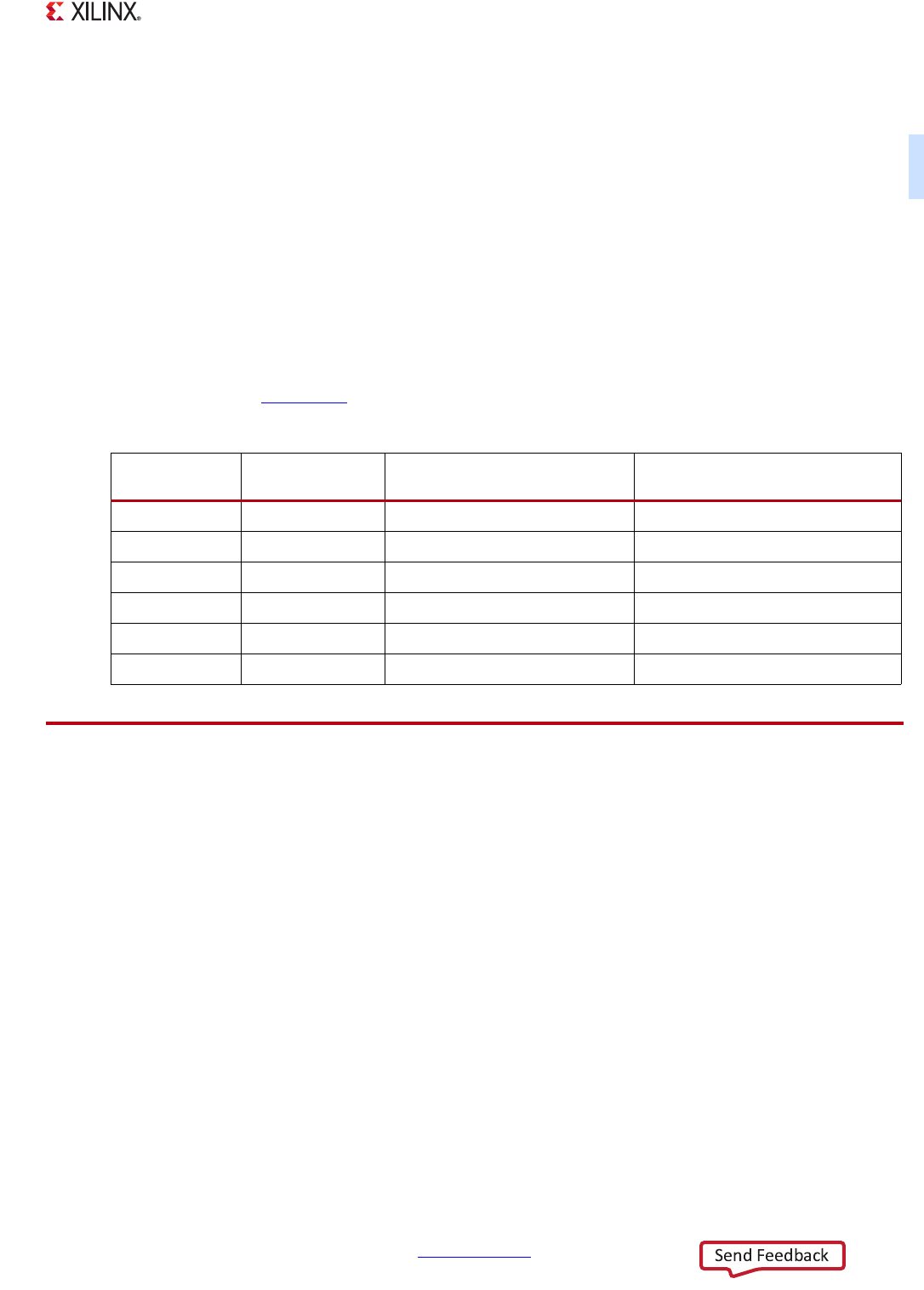
Table 11-1: MIO Pin 1 Programming for the NOR/SRAM Controller
slcr.MIO_PIN_01
{L2_SEL}
Address Accessed MIO0 MIO1
01 (ADDR25) 0xe200_0000 1->0->1 (acts as active CS0) 1 (acts as inverted ADDR25)
01 (ADDR25) 0xe400_0000
0 (acts as inactive CS0) 0 (acts as inverted ADDR25)
10 (CS1) 0xe200_0000
1->0->1 (acts as active CS0) 1 (acts as inactive CS1)
10 (CS1) 0xe400_0000
1 (acts as inactive CS0) 1->0->1 (acts as active CS1)
00 (GPIO) 0xe200_0000
1->0->1 (acts as active CS0) 1 (reset state, internal pull-up)
00 (GPIO) 0xe400_0000
1 (acts as inactive CS0) 1 (reset state, internal pull-up)