
User manual


Table Of Contents
- Zynq-7000 All Programmable SoC
- Table of Contents
- Ch. 1: Introduction
- Ch. 2: Signals, Interfaces, and Pins
- Ch. 3: Application Processing Unit
- Ch. 4: System Addresses
- Ch. 5: Interconnect
- Ch. 6: Boot and Configuration
- Ch. 7: Interrupts
- Ch. 8: Timers
- Ch. 9: DMA Controller
- Introduction
- Functional Description
- DMA Transfers on the AXI Interconnect
- AXI Transaction Considerations
- DMA Manager
- Multi-channel Data FIFO (MFIFO)
- Memory-to-Memory Transfers
- PL Peripheral AXI Transactions
- PL Peripheral Request Interface
- PL Peripheral - Length Managed by PL Peripheral
- PL Peripheral - Length Managed by DMAC
- Events and Interrupts
- Aborts
- Security
- IP Configuration Options
- Programming Guide for DMA Controller
- Programming Guide for DMA Engine
- Programming Restrictions
- System Functions
- I/O Interface
- Ch. 10: DDR Memory Controller
- Introduction
- AXI Memory Port Interface (DDRI)
- DDR Core and Transaction Scheduler (DDRC)
- DDRC Arbitration
- Controller PHY (DDRP)
- Initialization and Calibration
- DDR Clock Initialization
- DDR IOB Impedance Calibration
- DDR IOB Configuration
- DDR Controller Register Programming
- DRAM Reset and Initialization
- DRAM Input Impedance (ODT) Calibration
- DRAM Output Impedance (RON) Calibration
- DRAM Training
- Write Data Eye Adjustment
- Alternatives to Automatic DRAM Training
- DRAM Write Latency Restriction
- Register Overview
- Error Correction Code (ECC)
- Programming Model
- Ch. 11: Static Memory Controller
- Ch. 12: Quad-SPI Flash Controller
- Ch. 13: SD/SDIO Controller
- Ch. 14: General Purpose I/O (GPIO)
- Ch. 15: USB Host, Device, and OTG Controller
- Introduction
- Functional Description
- Programming Overview and Reference
- Device Mode Control
- Device Endpoint Data Structures
- Device Endpoint Packet Operational Model
- Device Endpoint Descriptor Reference
- Programming Guide for Device Controller
- Programming Guide for Device Endpoint Data Structures
- Host Mode Data Structures
- EHCI Implementation
- Host Data Structures Reference
- Programming Guide for Host Controller
- OTG Description and Reference
- System Functions
- I/O Interfaces
- Ch. 16: Gigabit Ethernet Controller
- Ch. 17: SPI Controller
- Ch. 18: CAN Controller
- Ch. 19: UART Controller
- Ch. 20: I2C Controller
- Ch. 21: Programmable Logic Description
- Ch. 22: Programmable Logic Design Guide
- Ch. 23: Programmable Logic Test and Debug
- Ch. 24: Power Management
- Ch. 25: Clocks
- Ch. 26: Reset System
- Ch. 27: JTAG and DAP Subsystem
- Ch. 28: System Test and Debug
- Ch. 29: On-Chip Memory (OCM)
- Ch. 30: XADC Interface
- Ch. 31: PCI Express
- Ch. 32: Device Secure Boot
- Appx. A: Additional Resources
- Appx. B: Register Details
- Overview
- Acronyms
- Module Summary
- AXI_HP Interface (AFI) (axi_hp)
- CAN Controller (can)
- DDR Memory Controller (ddrc)
- CoreSight Cross Trigger Interface (cti)
- Performance Monitor Unit (cortexa9_pmu)
- CoreSight Program Trace Macrocell (ptm)
- Debug Access Port (dap)
- CoreSight Embedded Trace Buffer (etb)
- PL Fabric Trace Monitor (ftm)
- CoreSight Trace Funnel (funnel)
- CoreSight Intstrumentation Trace Macrocell (itm)
- CoreSight Trace Packet Output (tpiu)
- Device Configuration Interface (devcfg)
- DMA Controller (dmac)
- Gigabit Ethernet Controller (GEM)
- General Purpose I/O (gpio)
- Interconnect QoS (qos301)
- NIC301 Address Region Control (nic301_addr_region_ctrl_registers)
- I2C Controller (IIC)
- L2 Cache (L2Cpl310)
- Application Processing Unit (mpcore)
- On-Chip Memory (ocm)
- Quad-SPI Flash Controller (qspi)
- SD Controller (sdio)
- System Level Control Registers (slcr)
- Static Memory Controller (pl353)
- SPI Controller (SPI)
- System Watchdog Timer (swdt)
- Triple Timer Counter (ttc)
- UART Controller (UART)
- USB Controller (usb)
Zynq-7000 AP SoC Technical Reference Manual www.xilinx.com 331
UG585 (v1.11) September 27, 2016
Chapter 11: Static Memory Controller
TIP: For power management, the clock enable in the slcr register can be used to turn off the clock. The
operating frequency for the reference clock is defined in the data sheet. (Clock gating is used to stop the
clock to save power.)
11.2.3 Resets
The controller has two reset inputs that are controlled by the reset subsystem; refer to Chapter 26,
Reset System. This SMC CPU_1x reset is used for the AXI and APB interfaces. The SMC_Ref reset is for
the FIFOs and the rest of the controller including the control and status registers.
11.2.4 ECC Support
User code can determine if the NAND device includes on-chip ECC or not by reading the
manufacturer and device ID's in the flash device. The supported boot devices are listed in Xilinx
AR50991
. The vendor specifications for NAND device should be reviewed for ECC support. On-chip
ECC errors are flagged using the NAND Interrupt.
When a flash device does not support on-chip ECC, then the 1-bit ECC unit in the SMC controller can
be used. Refer to ARM PrimeCell Static Memory Controller (PL350 series) Technical Reference Manual,
Revision r2p1 for programming information. ECC errors detected by the SMC controller are flagged
with the ECC Interrupt.
When programming NAND, the SMC controller adds an inversion of the ECC code if the number of
ones (bits=1) in the ECC block (512 bytes = 4096 bits) is odd. To match the hardware behavior,
software should add an inversion of the ECC code if the number of ones (bits=1) in the ECC block
(512 bytes = 4096 bits) is even.
11.2.5 Interrupts
The controller includes three interrupt sources. These interrupts are controlled by the
smc.MEMC_STATUS register. When enabled, the interrupt generates the IRQ ID # 50 signal to the
system interrupt controller.
• NAND ECC is triggered by SMC ECC logic.
• NAND Interrupt is triggered on the rising edge of the NAND_BUSY input pin on MIO.
• SRAM Interrupt is triggered on the rising edge of the EMIOSRAMINTIN signal from PL.
The source of the interrupt is determined by reading the smc.MEMC_STATUS register.
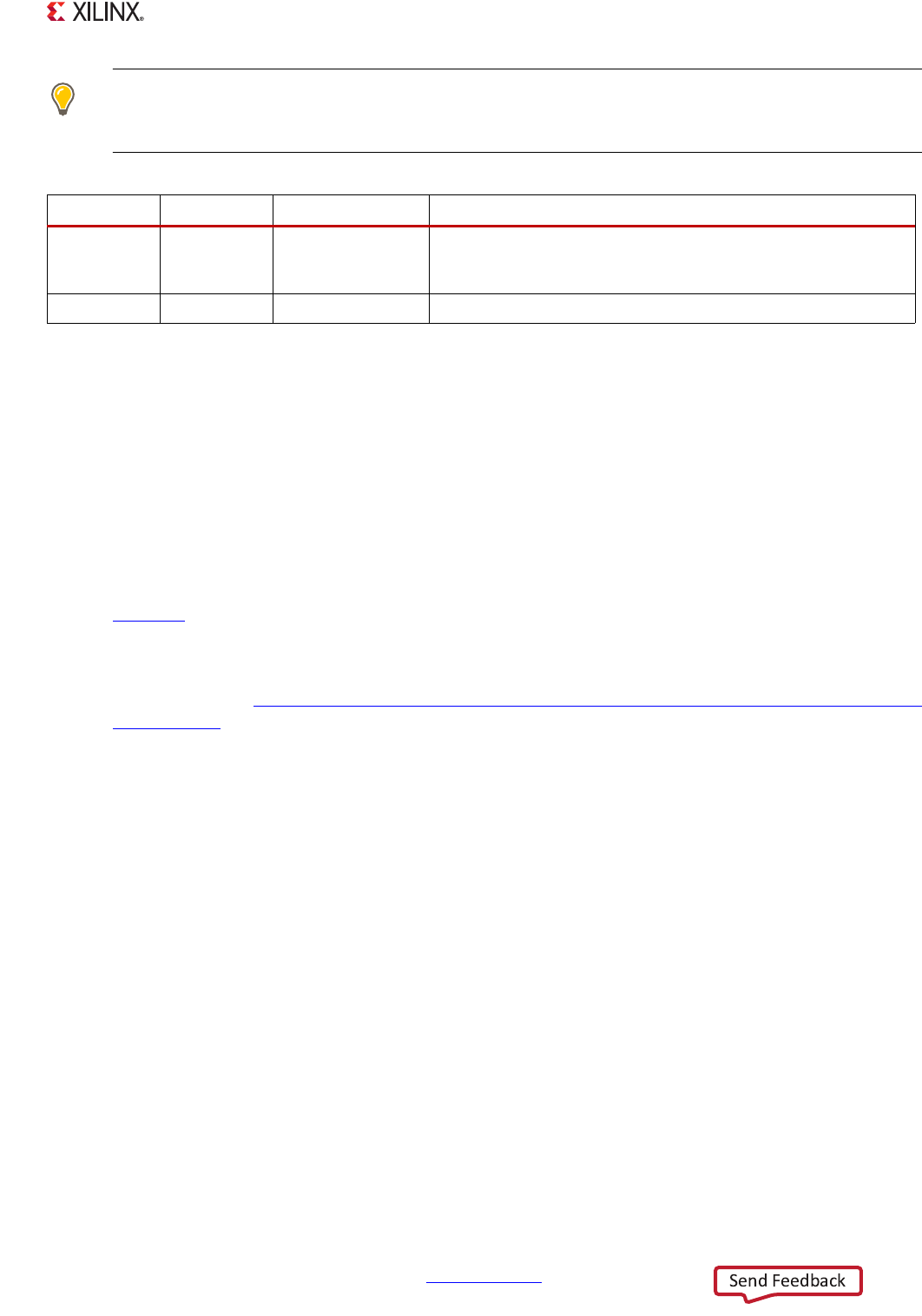
Table 11-2: SMC Clocks and Resets
Clock Resets Clock Domain Description
CPU_1x CPU_1x
Interconnect
domain
This clock runs at 1/6
th
or 1/4
th
the CPU clock rate depending on
the CPU clock mode. To stop this clock, first put the SMC is in
low-power mode.
SMC_Ref SMC_Ref SMC domain This clock is used to control the I/O memory interfaces.