
User manual


Table Of Contents
- Zynq-7000 All Programmable SoC
- Table of Contents
- Ch. 1: Introduction
- Ch. 2: Signals, Interfaces, and Pins
- Ch. 3: Application Processing Unit
- Ch. 4: System Addresses
- Ch. 5: Interconnect
- Ch. 6: Boot and Configuration
- Ch. 7: Interrupts
- Ch. 8: Timers
- Ch. 9: DMA Controller
- Introduction
- Functional Description
- DMA Transfers on the AXI Interconnect
- AXI Transaction Considerations
- DMA Manager
- Multi-channel Data FIFO (MFIFO)
- Memory-to-Memory Transfers
- PL Peripheral AXI Transactions
- PL Peripheral Request Interface
- PL Peripheral - Length Managed by PL Peripheral
- PL Peripheral - Length Managed by DMAC
- Events and Interrupts
- Aborts
- Security
- IP Configuration Options
- Programming Guide for DMA Controller
- Programming Guide for DMA Engine
- Programming Restrictions
- System Functions
- I/O Interface
- Ch. 10: DDR Memory Controller
- Introduction
- AXI Memory Port Interface (DDRI)
- DDR Core and Transaction Scheduler (DDRC)
- DDRC Arbitration
- Controller PHY (DDRP)
- Initialization and Calibration
- DDR Clock Initialization
- DDR IOB Impedance Calibration
- DDR IOB Configuration
- DDR Controller Register Programming
- DRAM Reset and Initialization
- DRAM Input Impedance (ODT) Calibration
- DRAM Output Impedance (RON) Calibration
- DRAM Training
- Write Data Eye Adjustment
- Alternatives to Automatic DRAM Training
- DRAM Write Latency Restriction
- Register Overview
- Error Correction Code (ECC)
- Programming Model
- Ch. 11: Static Memory Controller
- Ch. 12: Quad-SPI Flash Controller
- Ch. 13: SD/SDIO Controller
- Ch. 14: General Purpose I/O (GPIO)
- Ch. 15: USB Host, Device, and OTG Controller
- Introduction
- Functional Description
- Programming Overview and Reference
- Device Mode Control
- Device Endpoint Data Structures
- Device Endpoint Packet Operational Model
- Device Endpoint Descriptor Reference
- Programming Guide for Device Controller
- Programming Guide for Device Endpoint Data Structures
- Host Mode Data Structures
- EHCI Implementation
- Host Data Structures Reference
- Programming Guide for Host Controller
- OTG Description and Reference
- System Functions
- I/O Interfaces
- Ch. 16: Gigabit Ethernet Controller
- Ch. 17: SPI Controller
- Ch. 18: CAN Controller
- Ch. 19: UART Controller
- Ch. 20: I2C Controller
- Ch. 21: Programmable Logic Description
- Ch. 22: Programmable Logic Design Guide
- Ch. 23: Programmable Logic Test and Debug
- Ch. 24: Power Management
- Ch. 25: Clocks
- Ch. 26: Reset System
- Ch. 27: JTAG and DAP Subsystem
- Ch. 28: System Test and Debug
- Ch. 29: On-Chip Memory (OCM)
- Ch. 30: XADC Interface
- Ch. 31: PCI Express
- Ch. 32: Device Secure Boot
- Appx. A: Additional Resources
- Appx. B: Register Details
- Overview
- Acronyms
- Module Summary
- AXI_HP Interface (AFI) (axi_hp)
- CAN Controller (can)
- DDR Memory Controller (ddrc)
- CoreSight Cross Trigger Interface (cti)
- Performance Monitor Unit (cortexa9_pmu)
- CoreSight Program Trace Macrocell (ptm)
- Debug Access Port (dap)
- CoreSight Embedded Trace Buffer (etb)
- PL Fabric Trace Monitor (ftm)
- CoreSight Trace Funnel (funnel)
- CoreSight Intstrumentation Trace Macrocell (itm)
- CoreSight Trace Packet Output (tpiu)
- Device Configuration Interface (devcfg)
- DMA Controller (dmac)
- Gigabit Ethernet Controller (GEM)
- General Purpose I/O (gpio)
- Interconnect QoS (qos301)
- NIC301 Address Region Control (nic301_addr_region_ctrl_registers)
- I2C Controller (IIC)
- L2 Cache (L2Cpl310)
- Application Processing Unit (mpcore)
- On-Chip Memory (ocm)
- Quad-SPI Flash Controller (qspi)
- SD Controller (sdio)
- System Level Control Registers (slcr)
- Static Memory Controller (pl353)
- SPI Controller (SPI)
- System Watchdog Timer (swdt)
- Triple Timer Counter (ttc)
- UART Controller (UART)
- USB Controller (usb)
Zynq-7000 AP SoC Technical Reference Manual www.xilinx.com 332
UG585 (v1.11) September 27, 2016
Chapter 11: Static Memory Controller
11.2.6 PL353 Functionality
The SMC is based on ARM's PL353 Primecell core and is hard-coded such that controller 0 can
operate in SRAM/NOR mode and controller 1 can operate in NAND flash mode. The SRAM/NOR or
NAND interface can be used in a system, but not both. The SRAM/NOR interface does not support
PSRAM. The NAND flash controller does not support wear leveling.
When referencing ARM documentation, for programming and other purposes, refer to the
implementation notes in Table 11-3.
11.2.7 Address Map
The registers and memory base address are listed in Table 11-4.
11.3 I/O Signals
The MIO pin assignments for SRAM/NOR and NAND flash connections are shown in Table 11-5. The
SMC interface signals are routed only to the MIO pins, they are not available on the EMIO interface.
The MIO pins and restrictions (no NOR/SRAM and only 8-bit NAND) are shown in the MIO table in
section 2.5.4 MIO-at-a-Glance Table.
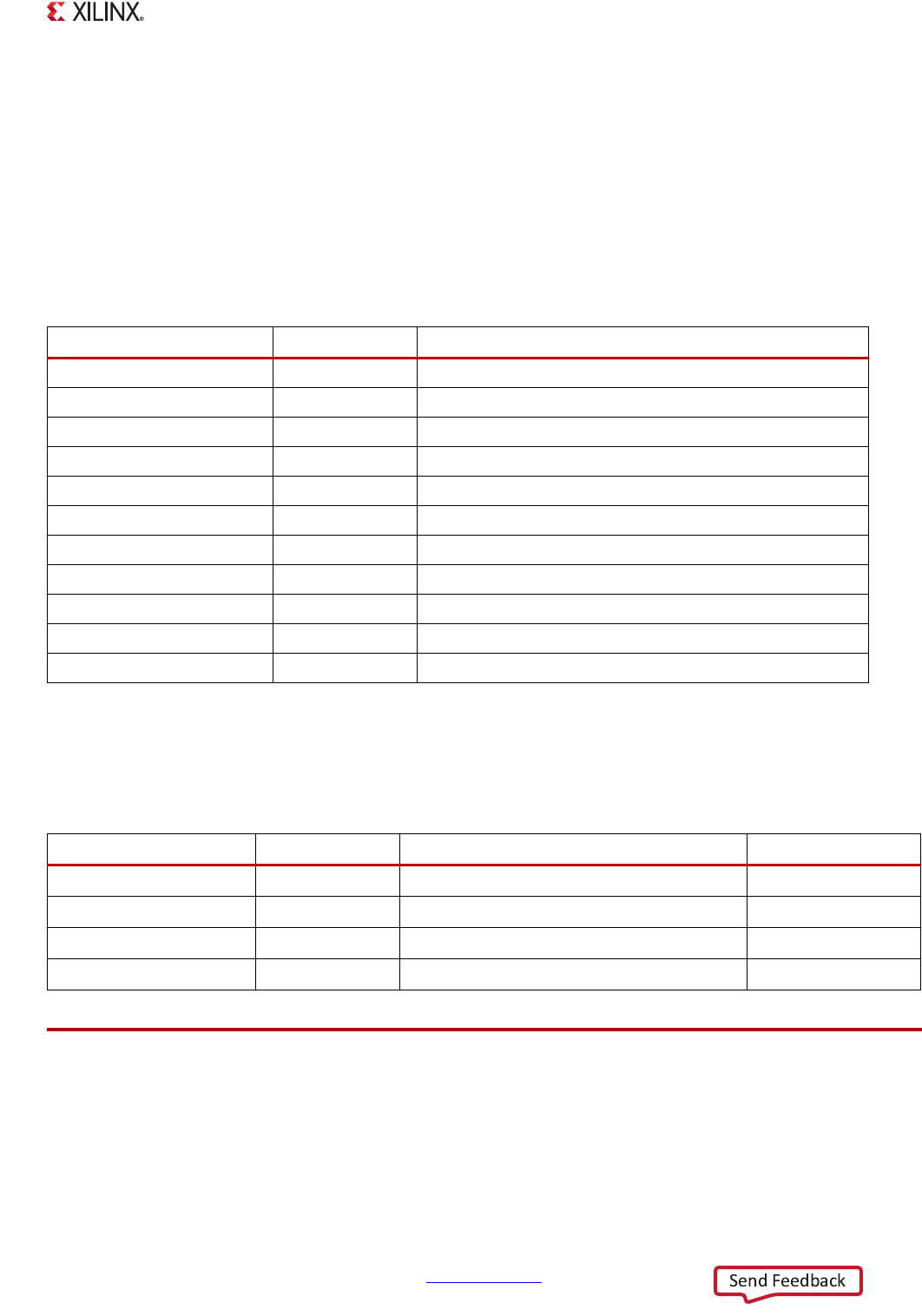
Table 11-3: SMC PL353 Implementation Notes
Parameter Value Design Notes
Chip Selects (Interface 0) 2 SRAM/NOR interface chip selects operate independently.
Chip Select (Interface 1) 1 NAND flash interface chip select
NAND flash mode data width 16 Data width can be 8 or 16 bits
SRAM mode data width 8 Data width is 8 bits.
System interface bus width 32 AXI
System interface clock rate ~ CPU_1x (1/6
th
or 1/4
th
the CPU clock frequency)
Command FIFO depth 8 Maximum supported depth on both interfaces
Read data word FIFO depth 16 Maximum supported depth on both interfaces
Write data word FIFO depth 16 Maximum supported depth on both interfaces
ECC support Yes 1-bit ECC hardware with assistance from software
ECC Extra Block Yes Supported
Table 11-4: SMC Address Map Summary
Base Address Mnemonic Description Type
0xE000_E000
SMC Configuration registers base address Registers
0xE100_0000
SMC_NAND SMC NAND memory base address Memory
0xE200_0000
SMC_SRAM0 SMC SRAM Chip Select 0 base address Memory
0xE400_0000
SMC_SRAM1 SMC SRAM Chip Select 1 base address Memory