
User manual


Table Of Contents
- Zynq-7000 All Programmable SoC
- Table of Contents
- Ch. 1: Introduction
- Ch. 2: Signals, Interfaces, and Pins
- Ch. 3: Application Processing Unit
- Ch. 4: System Addresses
- Ch. 5: Interconnect
- Ch. 6: Boot and Configuration
- Ch. 7: Interrupts
- Ch. 8: Timers
- Ch. 9: DMA Controller
- Introduction
- Functional Description
- DMA Transfers on the AXI Interconnect
- AXI Transaction Considerations
- DMA Manager
- Multi-channel Data FIFO (MFIFO)
- Memory-to-Memory Transfers
- PL Peripheral AXI Transactions
- PL Peripheral Request Interface
- PL Peripheral - Length Managed by PL Peripheral
- PL Peripheral - Length Managed by DMAC
- Events and Interrupts
- Aborts
- Security
- IP Configuration Options
- Programming Guide for DMA Controller
- Programming Guide for DMA Engine
- Programming Restrictions
- System Functions
- I/O Interface
- Ch. 10: DDR Memory Controller
- Introduction
- AXI Memory Port Interface (DDRI)
- DDR Core and Transaction Scheduler (DDRC)
- DDRC Arbitration
- Controller PHY (DDRP)
- Initialization and Calibration
- DDR Clock Initialization
- DDR IOB Impedance Calibration
- DDR IOB Configuration
- DDR Controller Register Programming
- DRAM Reset and Initialization
- DRAM Input Impedance (ODT) Calibration
- DRAM Output Impedance (RON) Calibration
- DRAM Training
- Write Data Eye Adjustment
- Alternatives to Automatic DRAM Training
- DRAM Write Latency Restriction
- Register Overview
- Error Correction Code (ECC)
- Programming Model
- Ch. 11: Static Memory Controller
- Ch. 12: Quad-SPI Flash Controller
- Ch. 13: SD/SDIO Controller
- Ch. 14: General Purpose I/O (GPIO)
- Ch. 15: USB Host, Device, and OTG Controller
- Introduction
- Functional Description
- Programming Overview and Reference
- Device Mode Control
- Device Endpoint Data Structures
- Device Endpoint Packet Operational Model
- Device Endpoint Descriptor Reference
- Programming Guide for Device Controller
- Programming Guide for Device Endpoint Data Structures
- Host Mode Data Structures
- EHCI Implementation
- Host Data Structures Reference
- Programming Guide for Host Controller
- OTG Description and Reference
- System Functions
- I/O Interfaces
- Ch. 16: Gigabit Ethernet Controller
- Ch. 17: SPI Controller
- Ch. 18: CAN Controller
- Ch. 19: UART Controller
- Ch. 20: I2C Controller
- Ch. 21: Programmable Logic Description
- Ch. 22: Programmable Logic Design Guide
- Ch. 23: Programmable Logic Test and Debug
- Ch. 24: Power Management
- Ch. 25: Clocks
- Ch. 26: Reset System
- Ch. 27: JTAG and DAP Subsystem
- Ch. 28: System Test and Debug
- Ch. 29: On-Chip Memory (OCM)
- Ch. 30: XADC Interface
- Ch. 31: PCI Express
- Ch. 32: Device Secure Boot
- Appx. A: Additional Resources
- Appx. B: Register Details
- Overview
- Acronyms
- Module Summary
- AXI_HP Interface (AFI) (axi_hp)
- CAN Controller (can)
- DDR Memory Controller (ddrc)
- CoreSight Cross Trigger Interface (cti)
- Performance Monitor Unit (cortexa9_pmu)
- CoreSight Program Trace Macrocell (ptm)
- Debug Access Port (dap)
- CoreSight Embedded Trace Buffer (etb)
- PL Fabric Trace Monitor (ftm)
- CoreSight Trace Funnel (funnel)
- CoreSight Intstrumentation Trace Macrocell (itm)
- CoreSight Trace Packet Output (tpiu)
- Device Configuration Interface (devcfg)
- DMA Controller (dmac)
- Gigabit Ethernet Controller (GEM)
- General Purpose I/O (gpio)
- Interconnect QoS (qos301)
- NIC301 Address Region Control (nic301_addr_region_ctrl_registers)
- I2C Controller (IIC)
- L2 Cache (L2Cpl310)
- Application Processing Unit (mpcore)
- On-Chip Memory (ocm)
- Quad-SPI Flash Controller (qspi)
- SD Controller (sdio)
- System Level Control Registers (slcr)
- Static Memory Controller (pl353)
- SPI Controller (SPI)
- System Watchdog Timer (swdt)
- Triple Timer Counter (ttc)
- UART Controller (UART)
- USB Controller (usb)
Zynq-7000 AP SoC Technical Reference Manual www.xilinx.com 342
UG585 (v1.11) September 27, 2016
Chapter 12: Quad-SPI Flash Controller
12.2.3 I/O Mode Transmit Registers (TXD)
Software writes byte sequences that are needed for the specific flash device. Refer to the Quad-SPI
device vendor's specification. The controller has four write-only 32-bit TXD registers for software to
issue a stream of commands to get status and read/write data from the flash memory. Quad-SPI TXD
register write formats are described in Table 12-1. Each access to the TXD0, TXD1, TXD2, or TXD3
register results into a corresponding write to the TxFIFO.
The user must empty the TxFIFO between consecutive accesses from:
• TXD0 to TXD1/TXD2/TXD3
• TXD1 to TXD0/TXD1/TXD2/TXD3
• TXD2 to TXD0/TXD1/TXD2/TXD3
• TXD3 to TXD0/TXD1/TXD2/TXD3
You need not empty the FIFO for TxD0 to TXD0 accesses.
FIFO Reads and Writes
The TxFIFO and RxFIFO share the same gated clock. Therefore for every byte, including command
and address bytes shifted out of the TxFIFO, a corresponding byte is shifted into the RxFIFO
To read data from Quad-SPI flash memory, the software writes the appropriate command, address,
mode (when in Quad or Dual I/O mode) and dummy cycles as required by the Quad-SPI flash
memory into the TxFIFO. In addition, software must pad the TxFIFO with additional dummy data. This
additional dummy data provides the CLK needed to shift data into the RxFIFO. See section
12.3.5 Rx/Tx FIFO Response to I/O Command Sequences for additional programming details.
12.2.4 I/O Mode Considerations
The RxFIFO interrupt status bit indicates when data is available before data is actually available for
read. The latency is associated with clock domain crossing and is almost always made-up by the time
that software takes to service the interrupt.
During a read command, software must write to the TxFIFO with dummy data to receive data from
the device. In automatic mode, if TxFIFO goes empty, the Quad-SPI controller deasserts chip select.
To further receive data, software must send the read command and address to the device.
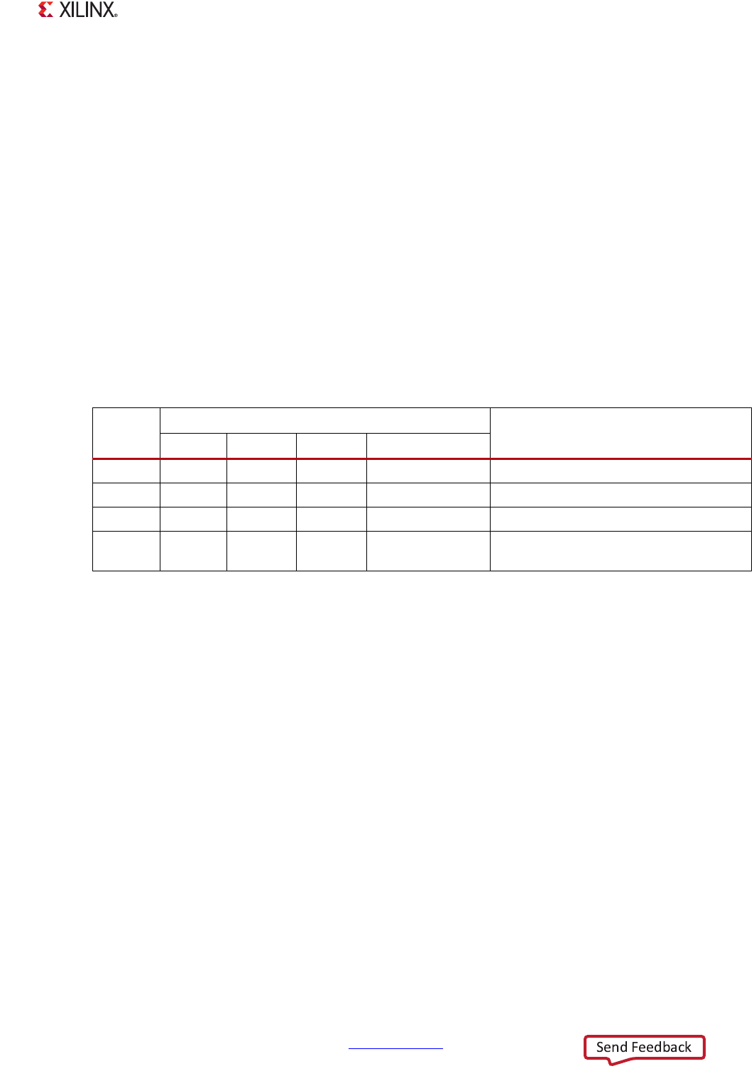
Table 12-1: Quad-SPI TXD Register Write Formats
Register
Write Data Format
Example Usage
31:24 23:16 15:8 7:0
TXD 1 Reserved Reserved Reserved Data or command Set write enable
TXD 2 Reserved Reserved Data 0 Data or command Write status with data
TXD 3 Reserved Data 1 Data 0 Data or command Read status with two dummy bytes
TXD 0 Data 3 Data 2 Data 1 Data or command Write data to transmit or dummy data for
reads