
User manual


Table Of Contents
- Zynq-7000 All Programmable SoC
- Table of Contents
- Ch. 1: Introduction
- Ch. 2: Signals, Interfaces, and Pins
- Ch. 3: Application Processing Unit
- Ch. 4: System Addresses
- Ch. 5: Interconnect
- Ch. 6: Boot and Configuration
- Ch. 7: Interrupts
- Ch. 8: Timers
- Ch. 9: DMA Controller
- Introduction
- Functional Description
- DMA Transfers on the AXI Interconnect
- AXI Transaction Considerations
- DMA Manager
- Multi-channel Data FIFO (MFIFO)
- Memory-to-Memory Transfers
- PL Peripheral AXI Transactions
- PL Peripheral Request Interface
- PL Peripheral - Length Managed by PL Peripheral
- PL Peripheral - Length Managed by DMAC
- Events and Interrupts
- Aborts
- Security
- IP Configuration Options
- Programming Guide for DMA Controller
- Programming Guide for DMA Engine
- Programming Restrictions
- System Functions
- I/O Interface
- Ch. 10: DDR Memory Controller
- Introduction
- AXI Memory Port Interface (DDRI)
- DDR Core and Transaction Scheduler (DDRC)
- DDRC Arbitration
- Controller PHY (DDRP)
- Initialization and Calibration
- DDR Clock Initialization
- DDR IOB Impedance Calibration
- DDR IOB Configuration
- DDR Controller Register Programming
- DRAM Reset and Initialization
- DRAM Input Impedance (ODT) Calibration
- DRAM Output Impedance (RON) Calibration
- DRAM Training
- Write Data Eye Adjustment
- Alternatives to Automatic DRAM Training
- DRAM Write Latency Restriction
- Register Overview
- Error Correction Code (ECC)
- Programming Model
- Ch. 11: Static Memory Controller
- Ch. 12: Quad-SPI Flash Controller
- Ch. 13: SD/SDIO Controller
- Ch. 14: General Purpose I/O (GPIO)
- Ch. 15: USB Host, Device, and OTG Controller
- Introduction
- Functional Description
- Programming Overview and Reference
- Device Mode Control
- Device Endpoint Data Structures
- Device Endpoint Packet Operational Model
- Device Endpoint Descriptor Reference
- Programming Guide for Device Controller
- Programming Guide for Device Endpoint Data Structures
- Host Mode Data Structures
- EHCI Implementation
- Host Data Structures Reference
- Programming Guide for Host Controller
- OTG Description and Reference
- System Functions
- I/O Interfaces
- Ch. 16: Gigabit Ethernet Controller
- Ch. 17: SPI Controller
- Ch. 18: CAN Controller
- Ch. 19: UART Controller
- Ch. 20: I2C Controller
- Ch. 21: Programmable Logic Description
- Ch. 22: Programmable Logic Design Guide
- Ch. 23: Programmable Logic Test and Debug
- Ch. 24: Power Management
- Ch. 25: Clocks
- Ch. 26: Reset System
- Ch. 27: JTAG and DAP Subsystem
- Ch. 28: System Test and Debug
- Ch. 29: On-Chip Memory (OCM)
- Ch. 30: XADC Interface
- Ch. 31: PCI Express
- Ch. 32: Device Secure Boot
- Appx. A: Additional Resources
- Appx. B: Register Details
- Overview
- Acronyms
- Module Summary
- AXI_HP Interface (AFI) (axi_hp)
- CAN Controller (can)
- DDR Memory Controller (ddrc)
- CoreSight Cross Trigger Interface (cti)
- Performance Monitor Unit (cortexa9_pmu)
- CoreSight Program Trace Macrocell (ptm)
- Debug Access Port (dap)
- CoreSight Embedded Trace Buffer (etb)
- PL Fabric Trace Monitor (ftm)
- CoreSight Trace Funnel (funnel)
- CoreSight Intstrumentation Trace Macrocell (itm)
- CoreSight Trace Packet Output (tpiu)
- Device Configuration Interface (devcfg)
- DMA Controller (dmac)
- Gigabit Ethernet Controller (GEM)
- General Purpose I/O (gpio)
- Interconnect QoS (qos301)
- NIC301 Address Region Control (nic301_addr_region_ctrl_registers)
- I2C Controller (IIC)
- L2 Cache (L2Cpl310)
- Application Processing Unit (mpcore)
- On-Chip Memory (ocm)
- Quad-SPI Flash Controller (qspi)
- SD Controller (sdio)
- System Level Control Registers (slcr)
- Static Memory Controller (pl353)
- SPI Controller (SPI)
- System Watchdog Timer (swdt)
- Triple Timer Counter (ttc)
- UART Controller (UART)
- USB Controller (usb)
Zynq-7000 AP SoC Technical Reference Manual www.xilinx.com 344
UG585 (v1.11) September 27, 2016
Chapter 12: Quad-SPI Flash Controller
AXI Read Command Processing
AXI read burst commands are translated into SPI flash read instructions that are sent to the Quad-SPI
controller TxFIFO. The controller transmit logic is responsible for retrieving the read instructions from
the FIFO and passing them along to the SPI flash memory according to the SPI protocol.
A 64-deep FIFO is used to provide read data buffering to hold up to four burst-of-16 data. Since the
Rx FIFO starts receiving data as soon as the chip-select signal is active, the linear address module
removes incoming data that corresponds to the instruction code, if any, the address, the dummy
cycles, and responses to the AXI read instruction with valid data.
Interface Configuration and Read Modes
AXI read burst transfers are translated into SPI flash read instructions that are sent to the controller's
TxFIFO. The transmit logic retrieves the read instructions from the TxFIFO and passes them to the SPI
flash memory device according to the SPI protocol.
Software defines the SPI read command that is used in linear addressing mode by writing to
qspi.LQSPI_CFG[INST_CODE]. The supported read command codes and the recommended
configuration register settings (qspi.LQSPI_CFG) are listed in Table 12-3. The optimal register values
for Quad-SPI boot performance using a 33 MHz PS_CLK are shown in Table 6-10 and Table 12-3.
These Quad-SPI registers can be programmed in non-secure mode using the Register Initialization
feature in the BootROM header to speed up loading of the FSBL/User code. If a faster PS_CLK is used,
then the clock dividers need to be adjusted.
The choice of operating mode depends on the capabilities of the attached device. The I/O Fast Read
modes use 4-bit parallel transfers for address and data. This leads to the fastest performance. The
Output Fast Read modes use 4-bit parallel transfers for data only. These are still faster than a serial
bit mode.
Performance Modes
To get the highest performance, the user should use the Quad-SPI controller in the Quad I/O mode.
The user can improve read performance by using the Quad-SPI device in continuous read mode.
This eliminates read instruction overhead for successive commands. Please refer to the LQSPI_CFG
register for more details (see Appendix B, Register Details).
Refer to the applicable Zynq-7000 AP SoC data sheet for operating frequencies.
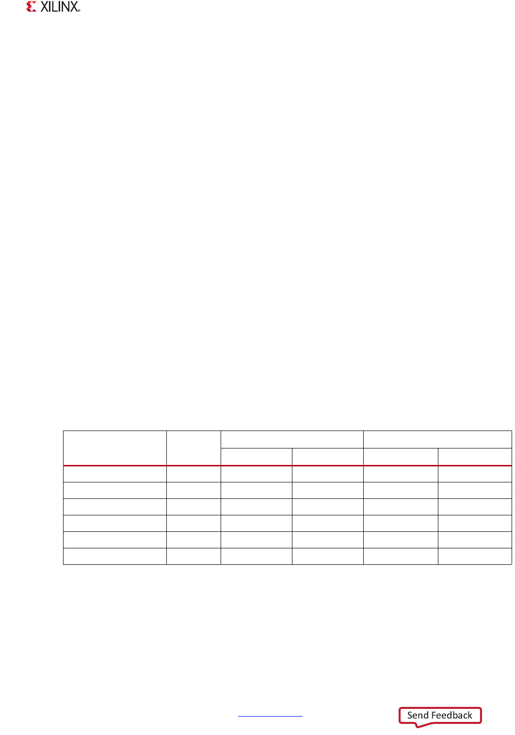
Table 12-3: Quad-SPI Device Configuration Register Values
Operating
Mode
Instruction
Code
Winbond & Spansion Micron
1 Device 2 Devices 1 Device 2 Devices
Read (serial bit) 0x03 0x80000003 0xE0000003 0x80000003 0xE0000003
Fast Read (serial bit) 0x0B 0x8000010B 0xE000010B 0x8000010B 0xE000010B
Dual Output Fast Read 0x3B 0x8000013B 0xE000013B 0x8000013B 0xE000013B
Quad Output Fast Read 0x6B 0x8000016B 0xE000016B 0x8000016B 0xE000016B
Dual I/O Fast Read 0xBB 0x82FF00BB 0xE2FF00BB 0x82FF01BB 0xE2FF01BB
Quad I/O Fast Read 0xEB 0x82FF02EB 0xE2FF02EB 0x82FF04EB 0xE2FF06EB