
User manual


Table Of Contents
- Zynq-7000 All Programmable SoC
- Table of Contents
- Ch. 1: Introduction
- Ch. 2: Signals, Interfaces, and Pins
- Ch. 3: Application Processing Unit
- Ch. 4: System Addresses
- Ch. 5: Interconnect
- Ch. 6: Boot and Configuration
- Ch. 7: Interrupts
- Ch. 8: Timers
- Ch. 9: DMA Controller
- Introduction
- Functional Description
- DMA Transfers on the AXI Interconnect
- AXI Transaction Considerations
- DMA Manager
- Multi-channel Data FIFO (MFIFO)
- Memory-to-Memory Transfers
- PL Peripheral AXI Transactions
- PL Peripheral Request Interface
- PL Peripheral - Length Managed by PL Peripheral
- PL Peripheral - Length Managed by DMAC
- Events and Interrupts
- Aborts
- Security
- IP Configuration Options
- Programming Guide for DMA Controller
- Programming Guide for DMA Engine
- Programming Restrictions
- System Functions
- I/O Interface
- Ch. 10: DDR Memory Controller
- Introduction
- AXI Memory Port Interface (DDRI)
- DDR Core and Transaction Scheduler (DDRC)
- DDRC Arbitration
- Controller PHY (DDRP)
- Initialization and Calibration
- DDR Clock Initialization
- DDR IOB Impedance Calibration
- DDR IOB Configuration
- DDR Controller Register Programming
- DRAM Reset and Initialization
- DRAM Input Impedance (ODT) Calibration
- DRAM Output Impedance (RON) Calibration
- DRAM Training
- Write Data Eye Adjustment
- Alternatives to Automatic DRAM Training
- DRAM Write Latency Restriction
- Register Overview
- Error Correction Code (ECC)
- Programming Model
- Ch. 11: Static Memory Controller
- Ch. 12: Quad-SPI Flash Controller
- Ch. 13: SD/SDIO Controller
- Ch. 14: General Purpose I/O (GPIO)
- Ch. 15: USB Host, Device, and OTG Controller
- Introduction
- Functional Description
- Programming Overview and Reference
- Device Mode Control
- Device Endpoint Data Structures
- Device Endpoint Packet Operational Model
- Device Endpoint Descriptor Reference
- Programming Guide for Device Controller
- Programming Guide for Device Endpoint Data Structures
- Host Mode Data Structures
- EHCI Implementation
- Host Data Structures Reference
- Programming Guide for Host Controller
- OTG Description and Reference
- System Functions
- I/O Interfaces
- Ch. 16: Gigabit Ethernet Controller
- Ch. 17: SPI Controller
- Ch. 18: CAN Controller
- Ch. 19: UART Controller
- Ch. 20: I2C Controller
- Ch. 21: Programmable Logic Description
- Ch. 22: Programmable Logic Design Guide
- Ch. 23: Programmable Logic Test and Debug
- Ch. 24: Power Management
- Ch. 25: Clocks
- Ch. 26: Reset System
- Ch. 27: JTAG and DAP Subsystem
- Ch. 28: System Test and Debug
- Ch. 29: On-Chip Memory (OCM)
- Ch. 30: XADC Interface
- Ch. 31: PCI Express
- Ch. 32: Device Secure Boot
- Appx. A: Additional Resources
- Appx. B: Register Details
- Overview
- Acronyms
- Module Summary
- AXI_HP Interface (AFI) (axi_hp)
- CAN Controller (can)
- DDR Memory Controller (ddrc)
- CoreSight Cross Trigger Interface (cti)
- Performance Monitor Unit (cortexa9_pmu)
- CoreSight Program Trace Macrocell (ptm)
- Debug Access Port (dap)
- CoreSight Embedded Trace Buffer (etb)
- PL Fabric Trace Monitor (ftm)
- CoreSight Trace Funnel (funnel)
- CoreSight Intstrumentation Trace Macrocell (itm)
- CoreSight Trace Packet Output (tpiu)
- Device Configuration Interface (devcfg)
- DMA Controller (dmac)
- Gigabit Ethernet Controller (GEM)
- General Purpose I/O (gpio)
- Interconnect QoS (qos301)
- NIC301 Address Region Control (nic301_addr_region_ctrl_registers)
- I2C Controller (IIC)
- L2 Cache (L2Cpl310)
- Application Processing Unit (mpcore)
- On-Chip Memory (ocm)
- Quad-SPI Flash Controller (qspi)
- SD Controller (sdio)
- System Level Control Registers (slcr)
- Static Memory Controller (pl353)
- SPI Controller (SPI)
- System Watchdog Timer (swdt)
- Triple Timer Counter (ttc)
- UART Controller (UART)
- USB Controller (usb)
Zynq-7000 AP SoC Technical Reference Manual www.xilinx.com 345
UG585 (v1.11) September 27, 2016
Chapter 12: Quad-SPI Flash Controller
Read Data Management
A 63-deep RxFIFO provides read data buffering to hold a minimum of three AXI burst transfer
lengths of 16 bytes each. Since the RxFIFO starts receiving data as soon as the chip-select signal is
active, the linear address adapter removes incoming data that corresponds to the instruction code,
if any, the address, and the dummy cycles.
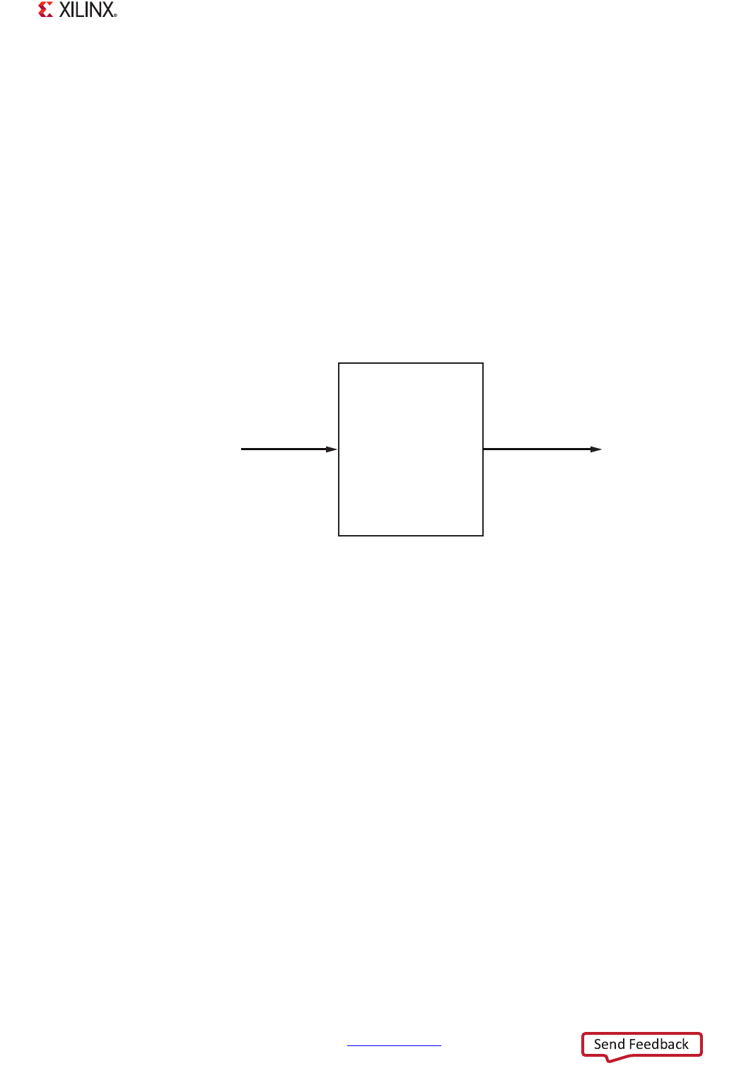
The read data must be aligned with the corresponding word boundary specified by the address. For
data alignment purposes, the controller can modify the address as illustrated in Figure 12-4 before
it is sent to the flash memory device. The address modification involves reducing the address by up
to 3 byte locations such that the intended return data is word aligned automatically. The amount of
address change is transparent to the AXI interface, and is instruction dependent.
For example, if Cmd + address + mode + dummy (QSPI_intruction) does not end on a 32 bit
boundary, the linear controller subtracts 1,2,3 from the address to align data on the 32 bit boundary.
Read Latency
In linear mode, the default read mode is fast Quad I/O. The following is an example to calculate latency
at the memory in the Quad I/O mode at 100 MHz with 2 dummy bytes. For a single device, the number
of clock cycles from the time an 8-bit instruction code and a 24-bit address is available to the time
when the first 32-bit data becomes available is:
Total latency = instruction latency + address latency + overhead (mode + dummy bites + offset) +
latency
= 8 cycles + 6 cycles + 8 (2+4+2) cycles + 8 cycles
=30 cycles
With the SPI clock of 100 MHz, the latency at the memory interface is 320 ns. Other read modes have
higher latency and can be calculated in a similar manner.
X-Ref Target - Figure 12-4
Figure 12-4: Automatic Address Offset For Word Alignment
UG585_c12_05_022712
Address Offset
Flash mem addr =
AXI read addr - x
Where x depends
on the instr type and
is either 0, 1, 2 or 3
AXI read addr
Flash mem addr